CY7C1303BV25
CY7C1306BV25
TAP AC Switching Characteristics Over the Operating Range[11, 12] (continued)
Parameter |
|
|
|
|
|
|
|
| Description |
|
|
|
|
| Min. | Max. | Unit | |||
Output Times |
|
|
|
|
|
|
|
|
|
|
|
|
|
|
|
|
| |||
tTDOV |
| TCK Clock LOW to TDO Valid |
|
|
|
|
|
| 20 | ns | ||||||||||
tTDOX |
| TCK Clock LOW to TDO Invalid |
|
|
|
|
| 0 |
| ns | ||||||||||
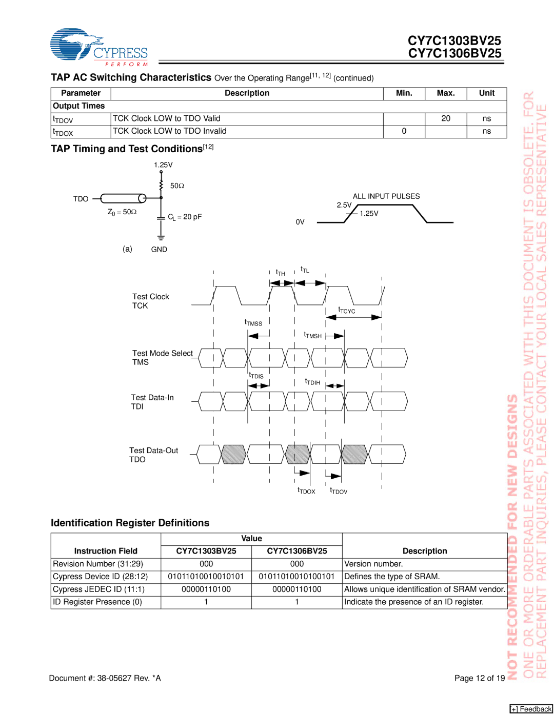
TAP Timing and Test Conditions[12] |
|
|
|
|
|
|
|
| ||||||||||||
|
|
|
|
|
| 1.25V |
|
|
|
|
|
|
|
| ||||||
|
|
|
|
|
|
|
|
|
|
|
| 50Ω |
|
|
| ALL INPUT PULSES |
|
| ||
|
|
|
|
|
|
|
|
|
|
|
|
|
|
|
|
| ||||
|
|
|
|
|
|
|
|
|
|
|
|
|
|
|
|
| ||||
|
|
|
|
|
|
|
|
|
|
|
|
|
|
|
|
|
| |||
|
|
|
|
|
|
|
|
|
|
|
|
|
|
| ||||||
TDO |
|
|
|
|
|
|
|
|
|
|
| |||||||||
|
|
|
|
|
|
|
|
|
| 2.5V |
|
| ||||||||
|
|
|
| Z0 = 50Ω |
|
|
|
|
|
|
|
|
|
| ||||||
|
|
|
|
|
|
|
|
|
| CL = 20 pF | 0V |
|
|
| 1.25V |
|
| |||
|
|
|
|
|
|
|
|
|
|
|
|
|
|
| ||||||
|
|
|
|
|
|
|
|
|
|
|
|
|
|
|
|
|
|
| ||
|
|
|
|
|
|
|
|
|
|
|
|
|
|
|
|
|
|
| ||
|
|
|
|
|
|
|
|
|
|
|
|
|
|
|
|
|
|
|
|
|
|
|
|
|
|
|
|
|
|
|
|
|
|
|
|
|
|
|
|
|
|
(a)GND
tTH
tTL
Test Clock
TCK
Test Mode Select
TMS
Test
TDI
![]()
![]()
![]() tTCYC tTMSS
tTCYC tTMSS ![]()
![]()
![]()
tTMSH
tTDIS
tTDIH
Test
TDO
tTDOX
tTDOV
Identification Register Definitions
| Value |
| |
Instruction Field | CY7C1303BV25 | CY7C1306BV25 | Description |
|
|
|
|
Revision Number (31:29) | 000 | 000 | Version number. |
|
|
|
|
Cypress Device ID (28:12) | 01011010010010101 | 01011010010100101 | Defines the type of SRAM. |
|
|
|
|
Cypress JEDEC ID (11:1) | 00000110100 | 00000110100 | Allows unique identification of SRAM vendor. |
|
|
|
|
ID Register Presence (0) | 1 | 1 | Indicate the presence of an ID register. |
|
|
|
|
Document #: | Page 12 of 19 |
[+] Feedback