CY7C1303BV25
CY7C1306BV25
operation is identical to the operation if the device had zero skew between the K/K and C/C clocks. All timing parameters remain the same in this mode. To use this mode of operation, the user must tie C and C HIGH at
Concurrent Transactions
The Read and Write ports on the CY7C1303BV25 operate completely independently of one another. Since each port latches the address inputs on different clock edges, the user can Read or Write to any location, regardless of the trans- action on the other port. Also, reads and writes can be started in the same clock cycle. If the ports access the same location at the same time, the SRAM will deliver the most recent infor- mation associated with the specified address location. This includes forwarding data from a Write cycle that was initiated on the previous K clock rise.
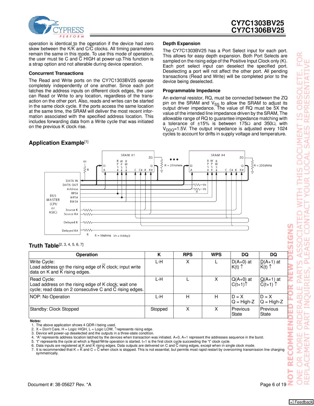
Application Example[1]
Depth Expansion
The CY7C1303BV25 has a Port Select input for each port. This allows for easy depth expansion. Both Port Selects are sampled on the rising edge of the Positive Input Clock only (K). Each port select input can deselect the specified port. Deselecting a port will not affect the other port. All pending transactions (Read and Write) will be completed prior to the device being deselected.
Programmable Impedance
An external resistor, RQ, must be connected between the ZQ pin on the SRAM and VSS to allow the SRAM to adjust its output driver impedance. The value of RQ must be 5X the value of the intended line impedance driven by the SRAM, The allowable range of RQ to guarantee impedance matching with a tolerance of ±15% is between 175Ω and 350Ω, with VDDQ=1.5V. The output impedance is adjusted every 1024 cycles to account for drifts in supply voltage and temperature.
Truth Table[2, 3, 4, 5, 6, 7]
Operation | K | RPS | WPS | DQ | DQ | ||
Write Cycle: | X | L | D(A+0) at | D(A+1) at | |||
Load address on the rising edge of | K | clock; input write |
|
|
| K(t) ↑ | K(t) ↑ |
data on K and K rising edges. |
|
|
|
|
| ||
Read Cycle: | L | X | Q(A+0) at | Q(A+1) at | |||
Load address on the rising edge of K clock; wait one |
|
|
| C(t+1)↑ | C(t+1) ↑ | ||
cycle; read data on 2 consecutive C and C rising edges. |
|
|
|
|
| ||
NOP: No Operation | H | H | D = X | D = X | |||
|
|
|
|
|
| Q = | Q = |
Standby: Clock Stopped | Stopped | X | X | Previous | Previous | ||
|
|
|
|
|
| State | State |
Notes:
1.The above application shows 4
2.X = Don't Care, H = Logic HIGH, L = Logic LOW, ↑represents rising edge.
3.Device will
4.“A” represents address location latched by the devices when transaction was initiated. A+0, A+1 represent the addresses sequence in the burst.
5.“t” represents the cycle at which a Read/Write operation is started. t+1 is the first clock cycle succeeding the “t” clock cycle.
6.Data inputs are registered at K and K rising edges. Data outputs are delivered on C and C rising edges, except when in single clock mode.
7.It is recommended that K = K and C = C when clock is stopped. This is not essential, but permits most rapid restart by overcoming transmission line charging symmetrically.
Document #: | Page 6 of 19 |
[+] Feedback