CY7C1303BV25
CY7C1306BV25
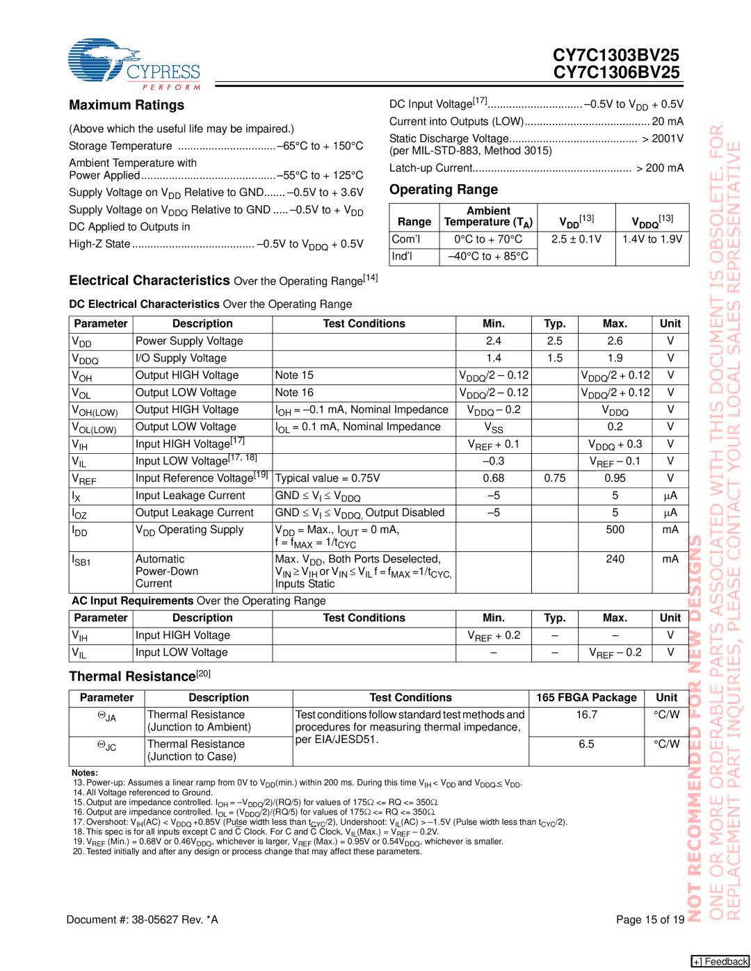
Maximum Ratings
(Above which the useful life may be impaired.)
Storage Temperature | ||
Ambient Temperature with |
|
|
Power Applied | ||
Supply Voltage on VDD Relative to GND | ||
Supply Voltage on VDDQ Relative to GND | ||
DC Applied to Outputs in |
|
|
|
| |
Electrical Characteristics Over the Operating Range[14] DC Electrical Characteristics Over the Operating Range
DC Input Voltage[17] |
| ||||
Current into Outputs (LOW) |
|
|
| 20 mA | |
Static Discharge Voltage |
|
|
| > 2001V | |
(per |
|
|
| ||
|
| > 200 mA | |||
Operating Range |
|
|
|
| |
|
|
|
|
|
|
Range | Ambient | V | [13] | V | [13] |
Temperature (T ) | |||||
| A |
| DD |
| DDQ |
Com’l | 0°C to + 70°C | 2.5 ± 0.1V | 1.4V to 1.9V | ||
|
|
|
|
|
|
Ind’l |
|
|
|
| |
|
|
|
|
|
|
Parameter |
|
| Description |
| Test Conditions | Min. | Typ. |
| Max. | Unit | ||
VDD |
| Power Supply Voltage |
|
| 2.4 |
| 2.5 |
| 2.6 |
| V | |
VDDQ |
| I/O Supply Voltage |
|
| 1.4 |
| 1.5 |
| 1.9 |
| V | |
VOH |
| Output HIGH Voltage | Note 15 | VDDQ/2 – 0.12 |
|
| VDDQ/2 + 0.12 | V | ||||
VOL |
| Output LOW Voltage | Note 16 | VDDQ/2 – 0.12 |
|
| VDDQ/2 + 0.12 | V | ||||
VOH(LOW) |
| Output HIGH Voltage | IOH = | VDDQ – 0.2 |
|
| VDDQ | V | ||||
VOL(LOW) |
| Output LOW Voltage | IOL = 0.1 mA, Nominal Impedance | VSS |
|
| 0.2 |
| V | |||
VIH |
| Input HIGH Voltage[17] |
|
| VREF + 0.1 |
|
| VDDQ + 0.3 | V | |||
VIL |
| Input LOW Voltage[17, 18] |
|
|
|
| VREF – 0.1 | V | ||||
VREF |
| Input Reference Voltage[19] | Typical value = 0.75V | 0.68 |
| 0.75 |
| 0.95 |
| V | ||
IX |
| Input Leakage Current | GND ≤ VI ≤ VDDQ |
|
| 5 |
| ∝A | ||||
IOZ |
| Output Leakage Current | GND ≤ VI ≤ VDDQ, Output Disabled |
|
| 5 |
| ∝A | ||||
IDD |
| VDD Operating Supply | VDD = Max., IOUT = 0 mA, |
|
|
|
| 500 |
| mA | ||
|
|
|
| f = fMAX = 1/tCYC |
|
|
|
|
|
|
| |
ISB1 |
| Automatic | Max. VDD, Both Ports Deselected, |
|
|
|
| 240 |
| mA | ||
|
| VIN ≥ VIH or VIN ≤ VIL f = fMAX =1/tCYC, |
|
|
|
|
|
|
| |||
|
| Current | Inputs Static |
|
|
|
|
|
|
| ||
AC Input | Requirements Over the Operating Range |
|
|
|
|
|
|
| ||||
|
|
|
|
|
|
|
|
|
|
|
|
|
Parameter |
|
| Description |
| Test Conditions | Min. | Typ. |
| Max. | Unit | ||
VIH |
| Input HIGH Voltage |
|
| VREF + 0.2 | – |
| – | V | |||
VIL |
| Input LOW Voltage |
|
| – | – |
| VREF – 0.2 | V | |||
Thermal Resistance[20] |
|
|
|
|
|
|
|
|
| |||
Parameter |
| Description |
| Test Conditions |
|
| 165 FBGA Package |
| Unit | |||
|
|
|
|
|
|
|
|
|
| |||
ΘJA |
| Thermal Resistance |
| Test conditions follow standard test methods and |
|
| 16.7 |
| °C/W | |||
|
|
| (Junction to Ambient) |
| procedures for measuring thermal impedance, |
|
|
|
|
|
| |
|
|
|
|
| per EIA/JESD51. |
|
|
|
|
|
|
|
ΘJC |
| Thermal Resistance |
|
|
|
| 6.5 |
| °C/W | |||
|
|
|
|
|
|
| ||||||
|
|
| (Junction to Case) |
|
|
|
|
|
|
|
|
|
Notes: |
|
|
|
|
|
|
|
|
|
|
| |
13.
14.All Voltage referenced to Ground.
15.Output are impedance controlled. IOH =
16.Output are impedance controlled. IOL = (VDDQ/2)/(RQ/5) for values of 175Ω <= RQ <= 350Ω.
17.Overshoot: VIH(AC) < VDDQ +0.85V (Pulse width less than tCYC/2), Undershoot: VIL(AC) >
18.This spec is for all inputs except C and C Clock. For C and C Clock, VIL(Max.) = VREF – 0.2V.
19.VREF (Min.) = 0.68V or 0.46VDDQ, whichever is larger, VREF (Max.) = 0.95V or 0.54VDDQ, whichever is smaller.
20.Tested initially and after any design or process change that may affect these parameters.
Document #: | Page 15 of 19 |
[+] Feedback
