|
|
|
|
|
|
| CY7C1303BV25 |
| |
|
|
|
|
|
|
| CY7C1306BV25 |
| |
|
|
|
|
|
|
|
|
|
|
Capacitance[23] |
|
|
|
|
| ||||
Parameter | Description | Test Conditions | Max. |
| Unit |
| |||
CIN | Input Capacitance | TA = 25°C, f = 1 MHz, | 5 |
| pF |
| |||
|
| VDD = 2.5V. |
|
|
|
| |||
CCLK | Clock Input Capacitance | 6 |
| pF |
| ||||
|
|
|
|
| VDDQ = 1.5V |
|
|
|
|
CO | Output Capacitance | 7 |
| pF |
| ||||
|
|
| |||||||
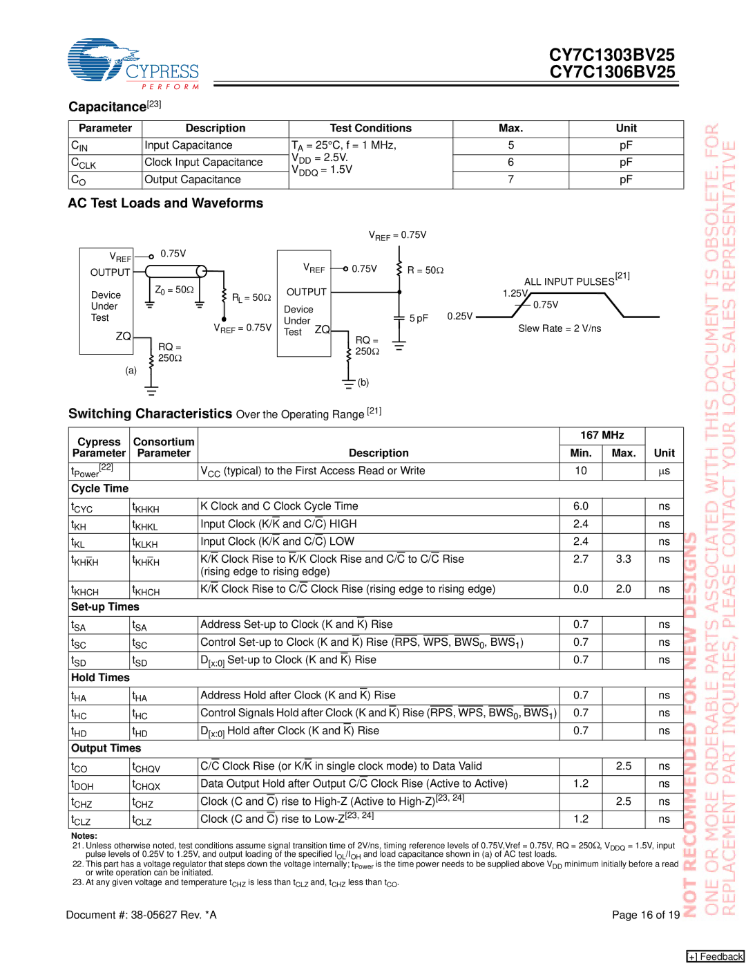
AC Test Loads and Waveforms
VREF = 0.75V
VREF |
|
|
|
|
|
|
| 0.75V |
|
| ||||
|
|
|
|
|
|
|
|
| ||||||
OUTPUT |
|
|
|
|
|
|
|
| Z0 = 50Ω |
|
| |||
|
|
|
|
|
|
|
|
|
| |||||
Device |
|
|
|
|
|
|
|
|
| |||||
Under |
|
|
|
|
|
|
|
|
|
|
|
|
| |
|
|
|
|
|
|
|
|
|
|
|
|
| ||
|
|
|
|
|
|
|
|
|
|
|
|
| ||
|
|
|
|
|
|
|
|
|
|
|
|
| ||
Test |
|
|
|
|
|
|
|
|
|
|
|
|
| |
ZQ
RQ =
![]()
![]() 250Ω
250Ω
(a)
![]()
![]() RL = 50Ω
RL = 50Ω
VREF = 0.75V
VREF |
|
|
| 0.75V |
|
|
| R = 50Ω | [21] | ||||||
|
|
|
|
| |||||||||||
|
|
|
|
| |||||||||||
OUTPUT |
|
|
|
|
|
|
|
|
|
| ALL INPUT PULSES | ||||
|
|
|
|
|
|
|
| 1.25V |
| ||||||
|
|
|
|
|
|
|
|
| |||||||
Device |
|
|
|
|
|
|
|
|
| 5 pF 0.25V |
|
|
| 0.75V |
|
|
|
|
|
|
|
|
|
|
|
|
|
| |||
|
|
|
|
|
|
|
|
|
|
|
|
|
| ||
Under | ZQ |
|
|
|
|
|
|
|
|
| Slew Rate = 2 V/ns |
| |||
|
|
|
|
|
|
|
|
| |||||||
|
|
|
|
|
|
|
|
|
| ||||||
Test |
|
| RQ = |
|
|
|
|
|
|
|
| ||||
|
|
|
|
|
|
|
|
| |||||||
|
|
|
|
|
|
|
|
|
| ||||||
|
|
|
|
|
|
|
|
|
|
|
|
|
|
| |
|
|
|
|
|
|
|
|
|
|
|
|
| |||
![]()
![]() 250Ω
250Ω
![]() (b)
(b)
Switching Characteristics Over the Operating Range [21]
Cypress | Consortium |
|
|
|
|
|
|
|
|
|
|
|
|
|
|
|
|
|
|
|
|
|
|
|
|
|
|
|
|
|
|
|
|
|
|
|
|
|
|
|
|
|
|
|
|
|
| 167 MHz |
| ||
Parameter |
| Parameter |
|
|
|
|
|
|
|
|
|
|
|
|
|
|
|
|
|
| Description | Min. | Max. | Unit | |||||||||||||||||||||||||||
tPower[22] |
|
| VCC (typical) to the First Access Read or Write | 10 |
| ∝s | |||||||||||||||||||||||||||||||||||||||||||||
Cycle Time |
|
|
|
|
|
|
|
|
|
|
|
|
|
|
|
|
|
|
|
|
|
|
|
|
|
|
|
|
|
|
|
|
|
|
|
|
|
|
|
|
|
|
|
|
|
|
|
|
|
|
|
|
|
|
|
|
| ||||||||||||||||||||||||||||||||||||||||||||||
tCYC | tKHKH | K Clock and C Clock Cycle Time | 6.0 |
| ns | ||||||||||||||||||||||||||||||||||||||||||||||
tKH | tKHKL | Input Clock (K/K | and C/C) HIGH | 2.4 |
| ns | |||||||||||||||||||||||||||||||||||||||||||||
tKL | tKLKH | Input Clock (K/K | and C/C) LOW | 2.4 |
| ns | |||||||||||||||||||||||||||||||||||||||||||||
tKHKH | tKHKH | K/K | Clock Rise to K/K Clock Rise and C/C to C/C Rise | 2.7 | 3.3 | ns | |||||||||||||||||||||||||||||||||||||||||||||
|
|
| (rising edge to rising edge) |
|
|
| |||||||||||||||||||||||||||||||||||||||||||||
tKHCH | tKHCH | K/K | Clock Rise to C/C Clock Rise (rising edge to rising edge) | 0.0 | 2.0 | ns | |||||||||||||||||||||||||||||||||||||||||||||
|
|
|
|
|
|
|
|
|
|
|
|
|
|
|
|
|
|
|
|
|
|
|
|
|
|
|
|
|
|
|
|
|
|
|
|
|
|
|
|
|
|
|
|
|
|
|
|
|
| ||
|
|
|
|
|
|
|
|
|
|
|
|
|
|
|
|
|
|
|
|
|
|
|
|
|
|
|
| ||||||||||||||||||||||||
tSA | tSA | Address | K) Rise | 0.7 |
| ns | |||||||||||||||||||||||||||||||||||||||||||||
tSC | tSC | Control | K) Rise (RPS, WPS, BWS0, BWS1) | 0.7 |
| ns | |||||||||||||||||||||||||||||||||||||||||||||
tSD | tSD | D[x:0] | K) Rise | 0.7 |
| ns | |||||||||||||||||||||||||||||||||||||||||||||
Hold Times |
|
|
|
|
|
|
|
|
|
|
|
|
|
|
|
|
|
|
|
|
|
|
|
|
|
|
|
|
|
|
|
|
|
|
|
|
|
|
|
|
|
|
|
|
|
|
|
|
|
|
|
|
|
|
|
|
|
|
|
|
|
|
|
|
|
|
|
|
| ||||||||||||||||||||||||||||||||||
tHA | tHA | Address Hold after Clock (K and | K) Rise | 0.7 |
| ns | |||||||||||||||||||||||||||||||||||||||||||||
tHC | tHC | Control Signals Hold after Clock (K and | K) Rise (RPS, WPS, BWS0, BWS1) | 0.7 |
| ns | |||||||||||||||||||||||||||||||||||||||||||||
tHD | tHD | D[x:0] Hold after Clock (K and | K) Rise | 0.7 |
| ns | |||||||||||||||||||||||||||||||||||||||||||||
Output Times |
|
|
|
|
|
|
|
|
|
|
|
|
|
|
|
|
|
|
|
|
|
|
|
|
|
|
|
|
|
|
|
|
|
|
|
|
|
|
|
|
|
|
|
|
|
|
|
|
| ||
|
|
|
|
|
|
|
|
|
| ||||||||||||||||||||||||||||||||||||||||||
tCO | tCHQV | C/C | Clock Rise (or K/K | in single clock mode) to Data Valid |
| 2.5 | ns | ||||||||||||||||||||||||||||||||||||||||||||
tDOH | tCHQX | Data Output Hold after Output C/C | Clock Rise (Active to Active) | 1.2 |
| ns | |||||||||||||||||||||||||||||||||||||||||||||
t | t | CHZ | Clock (C and | C) rise to |
| 2.5 | ns | ||||||||||||||||||||||||||||||||||||||||||||
CHZ |
|
|
|
|
|
|
|
|
|
|
|
|
|
|
|
|
|
|
|
|
|
|
|
|
|
|
|
|
|
|
|
|
|
|
|
|
|
|
|
|
|
|
|
|
|
|
|
|
|
| |
t | t | CLZ | Clock (C and | C) rise to | 1.2 |
| ns | ||||||||||||||||||||||||||||||||||||||||||||
CLZ |
|
|
|
|
|
|
|
|
|
|
|
|
|
|
|
|
|
|
|
|
|
|
|
|
|
|
|
|
|
|
|
|
|
|
|
|
|
|
|
|
|
|
|
|
|
|
|
|
|
| |
Notes:
21.Unless otherwise noted, test conditions assume signal transition time of 2V/ns, timing reference levels of 0.75V,Vref = 0.75V, RQ = 250Ω, VDDQ = 1.5V, input pulse levels of 0.25V to 1.25V, and output loading of the specified IOL/IOH and load capacitance shown in (a) of AC test loads.
22.This part has a voltage regulator that steps down the voltage internally; tPower is the time power needs to be supplied above VDD minimum initially before a read or write operation can be initiated.
23.At any given voltage and temperature tCHZ is less than tCLZ and, tCHZ less than tCO.
Document #: | Page 16 of 19 |
[+] Feedback