|
| PRELIMINARY |
|
|
|
|
|
| CY7C1333H | ||||||||
|
|
|
|
|
|
|
|
|
|
|
|
|
|
|
|
|
|
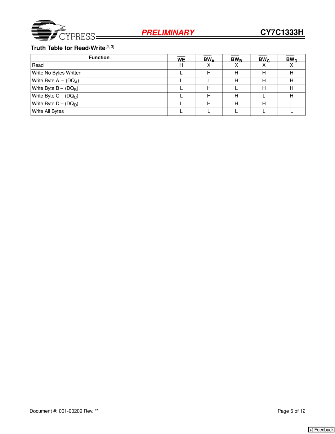
Truth Table for Read/Write[2, 3] |
|
|
|
|
|
|
|
|
|
|
|
|
|
|
|
| |
Function |
|
| WE |
| BWA |
| BWB |
| BWC |
| BWD | ||||||
|
|
|
|
|
|
|
| ||||||||||
Read |
|
| H |
| X |
| X |
| X |
| X | ||||||
|
|
|
|
|
|
|
|
|
|
|
| ||||||
Write No Bytes Written |
|
| L |
| H |
| H |
| H |
| H | ||||||
|
|
|
|
|
|
|
|
|
|
|
| ||||||
Write Byte A – (DQA) |
|
| L |
| L |
| H |
| H |
| H | ||||||
Write Byte B – (DQB) |
|
| L |
| H |
| L |
| H |
| H | ||||||
Write Byte C – (DQC) |
|
| L |
| H |
| H |
| L |
| H | ||||||
Write Byte D – (DQD) |
|
| L |
| H |
| H |
| H |
| L | ||||||
Write All Bytes |
|
| L |
| L |
| L |
| L |
| L | ||||||
|
|
|
|
|
|
|
|
|
|
|
|
|
|
|
|
|
|
Document #: | Page 6 of 12 |
[+] Feedback