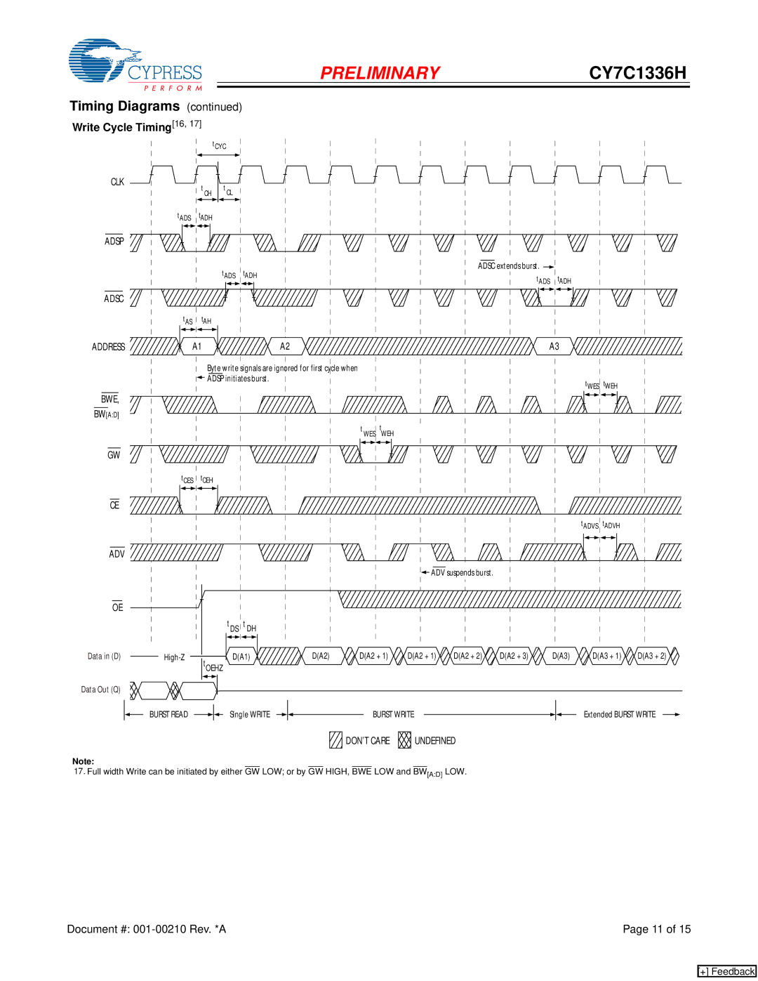
CY7C1336H specifications
The Cypress CY7C1336H is a high-performance static random-access memory (SRAM) device that has gained recognition for its outstanding speed and reliability. This component is widely used in various high-performance applications including networking, telecommunications, and industrial control systems, where fast data storage and retrieval are critical.One of the main features of the CY7C1336H is its high-speed operation, offering access times of as low as 10 nanoseconds. This makes it ideal for applications that require quick response times and efficient processing. The device operates with a supply voltage of 2.5V, which not only helps in reducing power consumption but also enables its use in newer low-voltage systems.
The CY7C1336H boasts a capacity of 1 megabit, organized in a configuration of 128K words by 8 bits. This allows it to store a significant amount of data while maintaining a compact footprint. In addition to its size, the device supports a burst mode, which enhances its efficiency in handling data transfer operations. This feature is particularly useful in applications requiring continuous data streaming, such as video processing or high-speed networking.
The memory technology employed in the CY7C1336H is known for its robustness and durability. Unlike DRAM, SRAM does not require periodic refreshing, which simplifies system design and improves overall performance. The device also features fast output enable and chip enable options, providing greater flexibility in controlling memory access and improving overall system response time.
In terms of packaging, the CY7C1336H is available in various forms including 32-pin SOJ and 44-pin TSOP packages, catering to diverse design requirements. Its compact packaging and low thermal characteristics make it suitable for space-constrained applications.
Another noteworthy characteristic of this SRAM is its inherent data integrity and reliability. With features such as on-chip parity generation and error checking capabilities, the CY7C1336H ensures that the data stored remains accurate and consistent over time.
Overall, the Cypress CY7C1336H delivers a blend of high speed, low power consumption, and reliability, making it an excellent choice for designers looking to implement high-performance memory solutions in their applications. Its combination of lasting performance and advanced features secures its place in both current and future electronic designs.

