CY7C1371DCY7C1373D
Document #: 38-05556 Rev. *F Page 13 of 29
boundary scan path when multiple devices are connected
together on a board.
EXTEST Output Bus Tri-State
IEEE Standard 1149.1 mandates that the TAP controller be
able to put the output bus into a tri-state mode.
The boundary scan register has a special bit located at bit #85
(for 119-BGA package) or bit #89 (for 165-fBGA package).
When this scan cell, called the “extest output bus tri-state,” is
latched into the preload register during the “Update-DR” state
in the TAP controller, it directly controls the state of the output
(Q-bus) pins, when the EXTEST is entered as the current
instruction. When HIGH, it enables the output buffers to drive
the output bus. When LOW, this bit places the output bus into
a High-Z condition.
This bit can be set by entering the SAMPLE/PRELOAD or
EXTEST command, and then shifting the desired bit into that
cell, during the “Shift-DR” state. During “Update-DR,” the value
loaded into that shift-register cell latches into the preload
register. When the EXTEST instruction is entered, this bit
directly controls the output Q-bus pins. Note that this bit is
preset HIGH to enable the output when the device is
powered-up, and also when the TAP controller is in the
“Test-Logic-Reset” state.
Reserved
These instructions are not implemented but are reserved for
future use. Do not use these instructions.
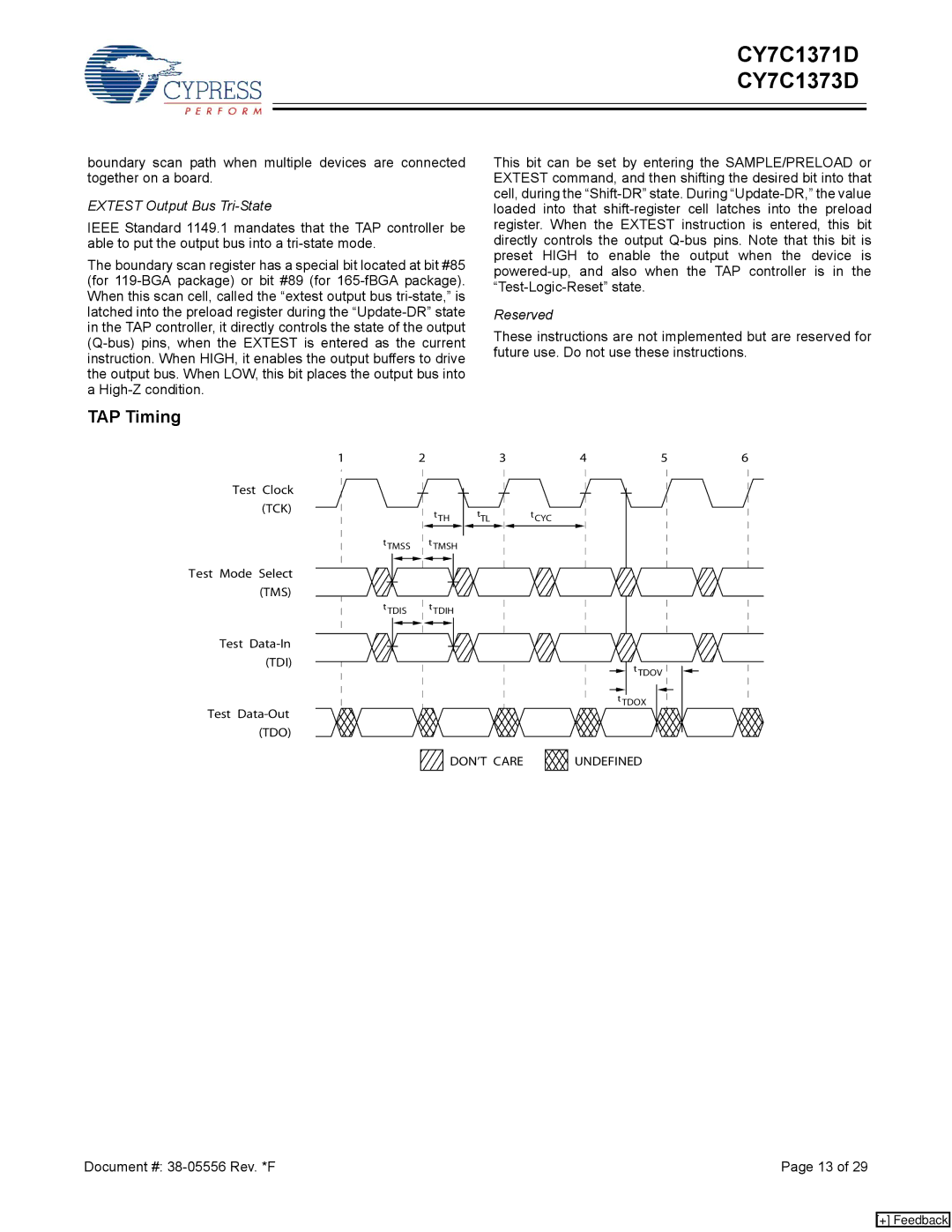
TAP Ti ming

tTL
Test Clock
(TCK)
123456
T
est Mode Select
(TMS)
tTH
Test Data-Out
(TDO)
tCYC
Test Data-In
(TDI)
tTMSH
tTMSS
tTDIH
tTDIS
tTDOX
tTDOV
DON’T CARE UNDEFINED
[+] Feedback