CY7C1371D
CY7C1373D
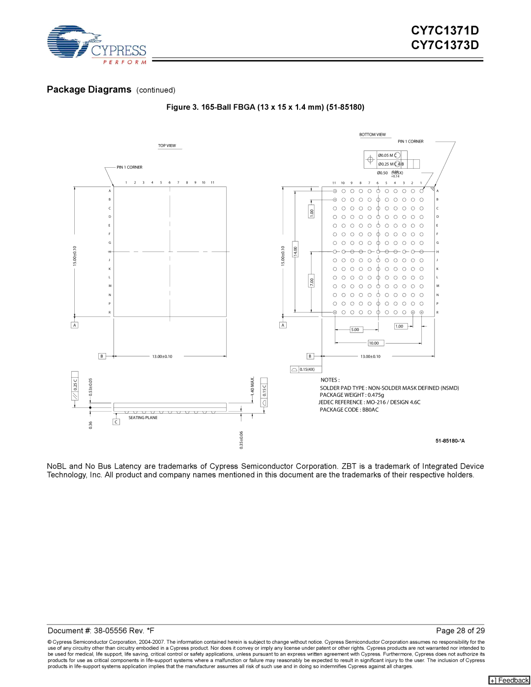
Package Diagrams (continued)
Figure 3. 165-Ball FBGA (13 x 15 x 1.4 mm) (51-85180)
15.00±0.10
TOP VIEW
PIN 1 CORNER
1 | 2 | 3 | 4 | 5 | 6 | 7 | 8 | 9 | 10 | 11 |
A
B
C
D
E
F
G
H
J
K
L
M
N
P
R
15.00±0.10
14.00
BOTTOM VIEW
PIN 1 CORNER
Ø0.05 M C Ø0.25 M C A B
Ø0.50 (165X)
+0.14
11 | 10 | 9 | 8 | 7 | 6 | 5 | 4 | 3 | 2 | 1 |
1.00
7.00
A
B
C
D
E
F
G
H
J
K
L
M
N
P
R
A
B
0.25 C | 0.53±0.05 |
| 0.36 |
13.00±0.10
SEATING PLANE
C
1.40MAX. |
| 0.15C |
|
|
|
|
|
|
0.35±0.06
A
1.00
5.00
10.00
B | 13.00±0.10 |
0.15(4X)
NOTES :
SOLDER PAD TYPE :
PACKAGE WEIGHT : 0.475g
JEDEC REFERENCE :
NoBL and No Bus Latency are trademarks of Cypress Semiconductor Corporation. ZBT is a trademark of Integrated Device Technology, Inc. All product and company names mentioned in this document are the trademarks of their respective holders.
Document #: | Page 28 of 29 |
© Cypress Semiconductor Corporation,
[+] Feedback