CY7C1371D
CY7C1373D
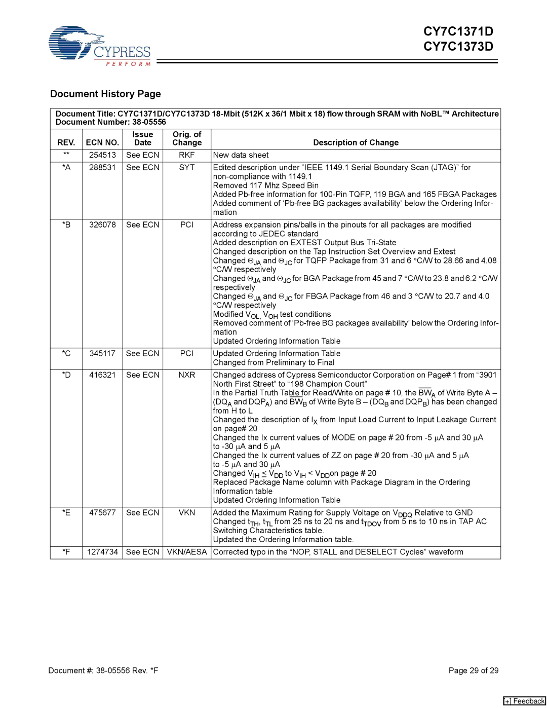
Document History Page
Document Title: CY7C1371D/CY7C1373D
Document Number:
REV. | ECN NO. | Issue | Orig. of | Description of Change | ||
Date | Change | |||||
|
|
|
|
| ||
** | 254513 | See ECN | RKF | New data sheet | ||
|
|
|
|
| ||
*A | 288531 | See ECN | SYT | Edited description under “IEEE 1149.1 Serial Boundary Scan (JTAG)” for | ||
|
|
|
| |||
|
|
|
| Removed 117 Mhz Speed Bin | ||
|
|
|
| Added | ||
|
|
|
| Added comment of | ||
|
|
|
| mation | ||
*B | 326078 | See ECN | PCI | Address expansion pins/balls in the pinouts for all packages are modified | ||
|
|
|
| according to JEDEC standard | ||
|
|
|
| Added description on EXTEST Output Bus | ||
|
|
|
| Changed description on the Tap Instruction Set Overview and Extest | ||
|
|
|
| Changed ΘJA and ΘJC for TQFP Package from 31 and 6 °C/W to 28.66 and 4.08 | ||
|
|
|
| °C/W respectively | ||
|
|
|
| Changed ΘJA and ΘJC for BGA Package from 45 and 7 °C/W to 23.8 and 6.2 °C/W | ||
|
|
|
| respectively | ||
|
|
|
| Changed ΘJA and ΘJC for FBGA Package from 46 and 3 °C/W to 20.7 and 4.0 | ||
|
|
|
| °C/W respectively | ||
|
|
|
| Modified VOL, VOH test conditions | ||
|
|
|
| Removed comment of | ||
|
|
|
| mation | ||
|
|
|
| Updated Ordering Information Table | ||
*C | 345117 | See ECN | PCI | Updated Ordering Information Table | ||
|
|
|
| Changed from Preliminary to Final | ||
*D | 416321 | See ECN | NXR | Changed address of Cypress Semiconductor Corporation on Page# 1 from “3901 | ||
|
|
|
| North First Street” to “198 Champion Court” | ||
|
|
|
| In the Partial Truth Table for Read/Write on page # 10, the | BW | A of Write Byte A – |
|
|
|
| (DQA and DQPA) and BWB of Write Byte B – (DQB and DQPB) has been changed | ||
|
|
|
| from H to L | ||
|
|
|
| Changed the description of IX from Input Load Current to Input Leakage Current | ||
|
|
|
| on page# 20 | ||
|
|
|
| Changed the Ix current values of MODE on page # 20 from | ||
|
|
|
| to | ||
|
|
|
| Changed the Ix current values of ZZ on page # 20 from | ||
|
|
|
| to | ||
|
|
|
| Changed VIH < VDD to VIH < VDDon page # 20 | ||
|
|
|
| Replaced Package Name column with Package Diagram in the Ordering | ||
|
|
|
| Information table | ||
|
|
|
| Updated Ordering Information Table | ||
*E | 475677 | See ECN | VKN | Added the Maximum Rating for Supply Voltage on VDDQ Relative to GND | ||
|
|
|
| Changed tTH, tTL from 25 ns to 20 ns and tTDOV from 5 ns to 10 ns in TAP AC | ||
|
|
|
| Switching Characteristics table. | ||
|
|
|
| Updated the Ordering Information table. | ||
*F | 1274734 | See ECN | VKN/AESA | Corrected typo in the “NOP, STALL and DESELECT Cycles” waveform | ||
|
|
|
|
|
|
|
Document #: | Page 29 of 29 |
[+] Feedback