CY7C138, CY7C139

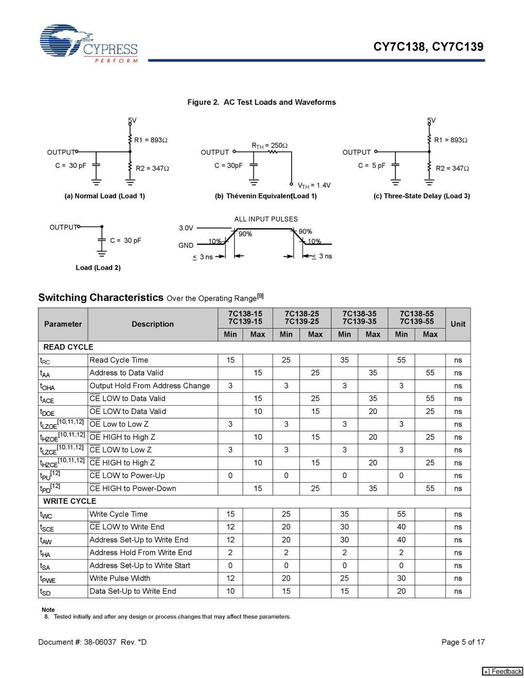
Figure 2. AC Test Loads and Waveforms

OUTPUT

C = 30 pF


5V


R1 = 893Ω


RTH = 250Ω


OUTPUT


R2 = 347Ω

C = 30pF


OUTPUT

C = 5 pF

VTH = 1.4V

5V

R1 = 893Ω

R2 = 347Ω

(a) Normal Load (Load 1)

(b) Thévenin Equivalent(Load 1)

(c) Three-State Delay (Load 3)

OUTPUT


C = 30 pF

3.0V


10%


GND


< 3 ns


Load (Load 2)


ALL INPUT PULSES

90%


90%


10%

< 3 ns

Switching Characteristics Over the Operating Range[9]


7C138-15

7C138-25

7C138-35

7C138-55


Parameter


Description

7C139-15

7C139-25

7C139-35

7C139-55

Unit


Min

Max

Min

Max

Min

Max

Min

Max


READ CYCLE


tRC


Read Cycle Time

15


25


35


55


ns

tAA


Address to Data Valid


15


25


35


55

ns

tOHA


Output Hold From Address Change

3


3


3


3


ns

tACE


LOW to Data Valid


15


25


35


55

ns

CE


tDOE


LOW to Data Valid


10


15


20


25

ns

OE


t

[10,11,12]


Low to Low Z

3


3


3


3


ns

OE


LZOE


t

[10,11,12]


HIGH to High Z


10


15


20


25

ns

OE


HZOE


t

[10,11,12]


LOW to Low Z

3


3


3


3


ns

CE


LZCE


t

[10,11,12]


HIGH to High Z


10


15


20


25

ns

CE


HZCE


t

[12]


LOW to Power-Up

0


0


0


0


ns

CE


PU


t

[12]


HIGH to Power-Down


15


25


35


55

ns

CE


PD


WRITE CYCLE


tWC


Write Cycle Time

15


25


35


55


ns

tSCE


LOW to Write End

12


20


30


40


ns

CE


tAW


Address Set-Up to Write End

12


20


30


40


ns

tHA


Address Hold From Write End

2


2


2


2


ns

tSA


Address Set-Up to Write Start

0


0


0


0


ns

tPWE


Write Pulse Width

12


20


25


30


ns

tSD


Data Set-Up to Write End

10


15


15


20


ns

Note

8. Tested initially and after any design or process changes that may affect these parameters.

Document #: 38-06037 Rev. *D

Page 5 of 17

[+] Feedback

Page 5
Image 5
Cypress CY7C139, CY7C138 manual Switching Characteristics Over the Operating Range9, Output, Gnd, ALL Input Pulses

CY7C138, CY7C139 specifications

The Cypress CY7C139 and CY7C138 are advanced static random-access memory (SRAM) components that have garnered attention in the field of digital electronics due to their high performance and reliability. These SRAMs are designed to meet the demanding needs of a variety of applications, ranging from telecommunications to automotive systems and consumer electronics.

The CY7C139 is a 128K x 8 bit static RAM, while the CY7C138 is a 256K x 8 bit SRAM, offering flexible memory solutions for designers. Both devices utilize a fast access time, typically around 10 to 15 nanoseconds, allowing quick data retrieval essential for high-speed applications. This remarkable speed is complemented by low power consumption, making them suitable for battery-operated devices and other applications where efficiency is paramount.

One of the key features of the CY7C139 and CY7C138 is their asynchronous operation, which enables them to provide high-speed data access without the need for a clock signal. This characteristic simplifies system design and enhances performance, as users can write to and read from the memory without waiting for synchronization. The devices support standard CMOS interface levels, which facilitate integration into a diverse range of digital systems.

Additionally, these SRAMs have been designed with a low standby current, making them particularly effective for low-power applications. The devices also include a robust input/output structure that ensures reliable signal integrity under various operating conditions. Their built-in data retention capability allows the SRAMs to retain stored data even during power failures, a critical feature in many systems that require data preservation.

Both CY7C139 and CY7C138 SRAMs support a wide range of temperature and voltage ranges, making them suitable for industrial and automotive environments. They are packaged in industry-standard configurations, allowing for easy integration into existing designs.

In summary, the Cypress CY7C139 and CY7C138 SRAMs provide high-speed, low-power memory solutions suitable for various applications. Their asynchronous operation, low standby current, and robust performance characteristics make them a preferred choice for engineers looking to enhance system efficiency and reliability. These features make the CY7C139 and CY7C138 indispensable components in modern digital electronic designs.