CY7C1381D, CY7C1381F

CY7C1383D, CY7C1383F

Package Diagrams (continued)

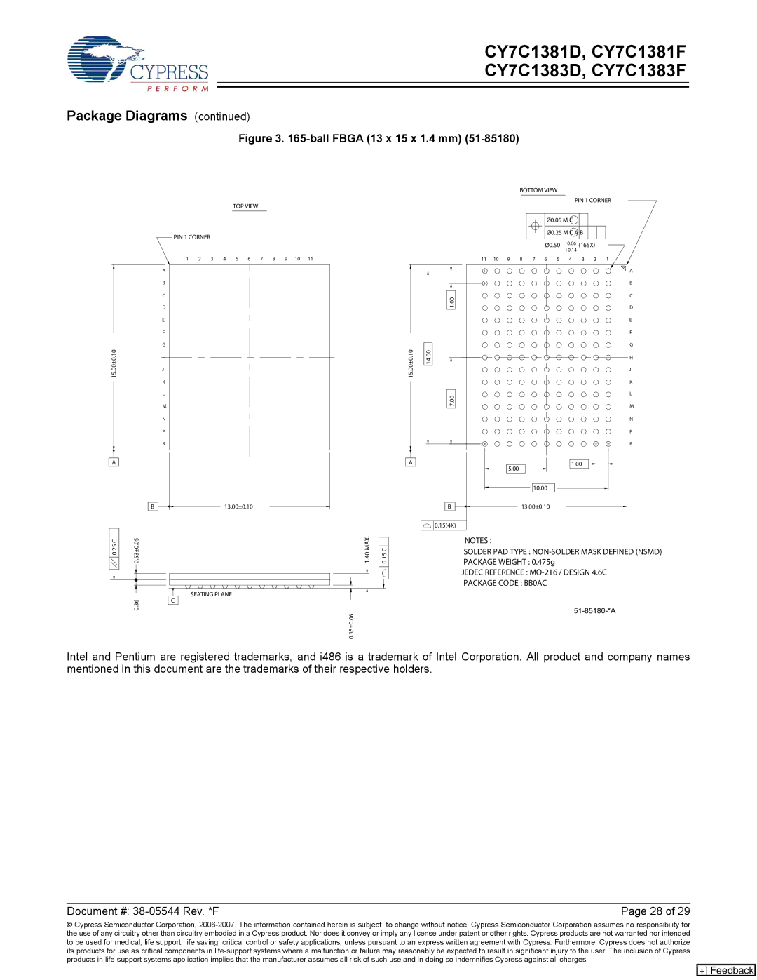
Figure 3. 165-ball FBGA (13 x 15 x 1.4 mm) (51-85180)

165 FBGA 13 x 15 x 1.40 MM BB165D/BW165D

TOP VIEW


TOP VIEW


PIN 1 CORNER


PIN 1 CORNER


1

2

3

4

5

6

7

8

9

10

11

BOTTOM VIEW

BOTTOM VIEWPIN 1 CORNER

PIN 1 CORNER


Ø0.05 M C


Ø0.05 M C


Ø0.25 M C A B


Ø0.50

-0.06Ø0.25 M C A B


(165X)


+0.14


-0.06


11

10

9

8

7

6

5

Ø0.50

(165X)

4

3

2

1


+0.14


A

1

2

3

4

5

6

7

8

9

10

11


BA

CB

DC

ED

FE

GF

15.00±0.10

15.00±0.10

H

G

15.00±0.10


J

H


K

J


LK

ML

NM

PN

RP

R

14.00

15.00±0.10

1.00

7.0014.00

1.00

7.00

11 10

9

8

7

6

5

4

3

2

A1

BA

CB

DC

ED

FE

GF

HG

JH

KJ

LK

ML

NM

PN

RP

R

A


A


A


B

13.00±0.10


B

13.00±0.10


C


1.40 MAX.


0.25C

0.53±0.05

0.53±0.05

0.15 C 1.40 MAX.

0.15 C

0.25


C

SEATING PLANE


0.36

SEATING PLANE


0.36

C


0.35±0.06

0.35±0.06


1.00

A

5.00

1.00


5.00


10.00


10.00

B

13.00±0.10

B

13.00±0.10

0.15(4X)


0.15(4X)


NOTES :


SOLDERNOTESPAD TYPE: : NON-SOLDER MASK DEFINED (NSMD)

PACKAGESOLDERWEIGHTPAD: 0TYPE.475g: NON-SOLDER MASK DEFINED (NSMD)

JEDEC REFERENCEPACKAGE WEIGHT: MO-216: 0/.475gDESIGN 4.6C

PACKAGEJEDECCODER FERENCE: BB0AC : MO-216 / DESIGN 4.6C

PACKAGE CODE : BB0AC

51-85180-*A

51-85180-*A

Intel and Pentium are registered trademarks, and i486 is a trademark of Intel Corporation. All product and company names mentioned in this document are the trademarks of their respective holders.

Document #: 38-05544 Rev. *F

Page 28 of 29

© Cypress Semiconductor Corporation, 2006-2007. The information contained herein is subject to change without notice. Cypress Semiconductor Corporation assumes no responsibility for the use of any circuitry other than circuitry embodied in a Cypress product. Nor does it convey or imply any license under patent or other rights. Cypress products are not warranted nor intended to be used for medical, life support, life saving, critical control or safety applications, unless pursuant to an express written agreement with Cypress. Furthermore, Cypress does not authorize its products for use as critical components in life-support systems where a malfunction or failure may reasonably be expected to result in significant injury to the user. The inclusion of Cypress products in life-support systems application implies that the manufacturer assumes all risk of such use and in doing so indemnifies Cypress against all charges.

[+] Feedback

Page 28
Image 28
Cypress CY7C1383F, CY7C1381D, CY7C1381F, CY7C1383D manual Soldernotespad Type NON-SOLDER Mask Defined Nsmd

CY7C1381D, CY7C1381F, CY7C1383D, CY7C1383F specifications

The Cypress CY7C1383F, CY7C1383D, CY7C1381F, and CY7C1381D are high-performance static random-access memory (SRAM) devices designed for a variety of applications requiring fast data storage and retrieval. These memory chips are part of the Cypress SRAM family, known for their low power consumption, high speed, and data integrity, making them suitable for use in telecommunications, networking, and industrial applications.

One of the standout features of the CY7C1383F and CY7C1383D models is their high density, offering 256K bits of memory. This provides ample space for storing critical data while maintaining excellent performance. The CY7C1381F and CY7C1381D variants, having a smaller capacity of 128K bits, are ideal for applications where space and power savings are paramount. All four devices are organized as 32K x 8 bits, promoting ease of integration into various designs.

These SRAM devices utilize advanced CMOS technology, which not only enhances their speed but also reduces power consumption. The fast access times, reaching as low as 10 nanoseconds for the CY7C1383F and CY7C1381F, enable high-speed data processing, making these memories suitable for cache applications and high-speed buffering. Overall, their performance characteristics ensure data can be accessed quickly and efficiently.

The CY7C1383F and CY7C1383D models come with an extended temperature range, ensuring consistent performance even in harsh environments. This reliability is critical for industrial applications where fluctuating temperatures can affect device functionality. Moreover, the CY7C1381F and CY7C1381D share this advantage, making all four components suitable for different operating conditions.

Built-in features such as byte-wide write enable and chip enable signals significantly ease the control of data access and manipulation. Additionally, the asynchronous nature of these SRAM devices allows for simple interfacing with various microcontrollers and processors, facilitating integration into existing systems with minimal design modifications.

In summary, the Cypress CY7C1383F, CY7C1383D, CY7C1381F, and CY7C1381D SRAM devices deliver high-performance data storage solutions, characterized by low power consumption, fast access times, and reliability in diverse operating conditions. Their versatility makes them an excellent choice for engineers seeking robust memory solutions in their designs.