CY7C1410AV18, CY7C1425AV18 CY7C1412AV18, CY7C1414AV18

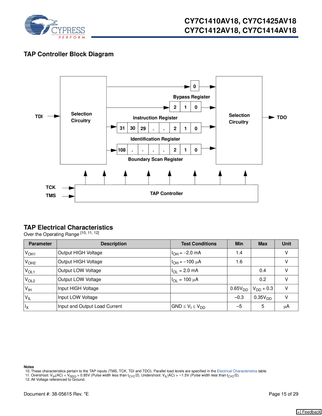
TAP Controller Block Diagram


0


Bypass Register


TDI


Selection


2

1

0


Selection


Instruction Register


Circuitry


Circuitry


31


30

29

.

.

2

1

0


Identification Register


108

.

.

.

.

2

1

0


Boundary Scan Register


TCK


TAP Controller


TMS


TDO

TAP Electrical Characteristics

Over the Operating Range [10, 11, 12]

Parameter

Description

Test Conditions

Min

Max

Unit

VOH1

Output HIGH Voltage

IOH = 2.0 mA

1.4


V

VOH2

Output HIGH Voltage

IOH = 100 μA

1.6


V

VOL1

Output LOW Voltage

IOL = 2.0 mA


0.4

V

VOL2

Output LOW Voltage

IOL = 100 μA


0.2

V

VIH

Input HIGH Voltage


0.65VDD

VDD + 0.3

V

VIL

Input LOW Voltage


–0.3

0.35VDD

V

IX

Input and Output Load Current

GND VI VDD

–5

5

μA

Notes

10.These characteristics pertain to the TAP inputs (TMS, TCK, TDI and TDO). Parallel load levels are specified in the Electrical Characteristics table.

11.Overshoot: VIH(AC) < VDDQ + 0.85V (Pulse width less than tCYC/2), Undershoot: VIL(AC) > 1.5V (Pulse width less than tCYC/2).

12.All Voltage referenced to Ground.

Document #: 38-05615 Rev. *E

Page 15 of 29

[+] Feedback

Page 15
Image 15
Cypress CY7C1412AV18, CY7C1410AV18 manual TAP Controller Block Diagram, TAP Electrical Characteristics, Tdi, Tck, Tms

CY7C1410AV18, CY7C1425AV18, CY7C1414AV18, CY7C1412AV18 specifications

Cypress Semiconductor, a prominent player in the semiconductor industry, offers a robust lineup of synchronous Static Random Access Memory (SRAM) products, including the CY7C1412AV18, CY7C1414AV18, CY7C1425AV18, and CY7C1410AV18. These memory chips are designed for high-performance applications, showcasing significant advancements in speed, density, and power efficiency.

The CY7C1412AV18 is a 1.2 Megabit SRAM with a 2.5V operating voltage. It boasts a maximum access time of 12 nanoseconds, specifically engineered for applications requiring fast data processing. This chip is particularly well-suited for networking and telecommunications applications where quick data retrieval is essential.

Next in the lineup, the CY7C1414AV18 offers a 1.44 Megabit capacity with a similar operating voltage and access time. This model's increased density allows for more data storage while maintaining performance levels, making it an excellent choice for automotive and industrial applications that demand reliability and speed.

Moreover, the CY7C1425AV18 is a more advanced solution with a 2 Megabit capacity. It integrates innovative features such as pipelined architecture, which enhances throughput and minimizes latency, making it ideal for high-speed processing applications like video and image processing in various electronic devices.

Lastly, the CY7C1410AV18 rounds out the series with a 1 Megabit capacity and is tailored for critical applications where space and power consumption are constraints. Its low power consumption makes it increasingly suitable for battery-operated devices, contributing to energy efficiency and extended operational life.

Each of these memory chips incorporates Cypress's advanced technology, including CMOS (Complementary Metal-Oxide-Semiconductor) fabrication processes, which ensures high performance while maintaining low static and dynamic power consumption. The SRAMs are designed with a 3.3V data interface, ensuring compatibility with modern digital systems.

In summary, Cypress's CY7C1412AV18, CY7C1414AV18, CY7C1425AV18, and CY7C1410AV18 SRAM chips stand out with their high access speeds, low power consumption, and varying capacities. These components are optimized for a wide range of applications, including networking, automotive, and consumer electronics, confirming Cypress's commitment to delivering cutting-edge memory solutions to meet the evolving demands of the electronics industry.