CY7C1410JV18, CY7C1425JV18
CY7C1412JV18, CY7C1414JV18
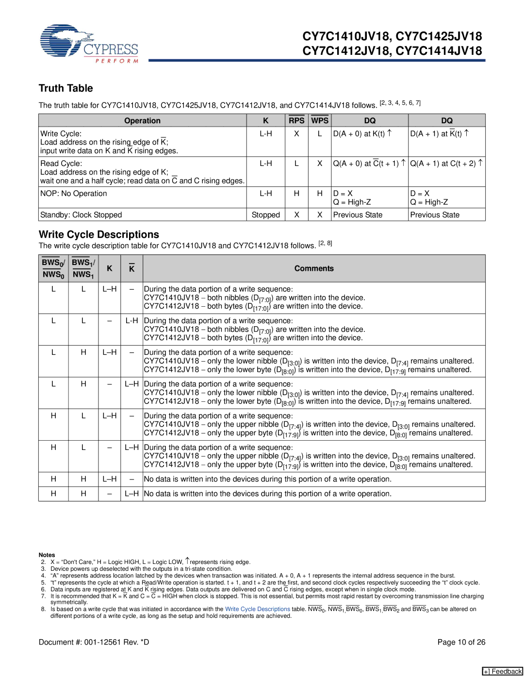
Truth Table
The truth table for CY7C1410JV18, CY7C1425JV18, CY7C1412JV18, and CY7C1414JV18 follows. [2, 3, 4, 5, 6, 7]
Operation | K | RPS |
|
| WPS | DQ | DQ | ||||||||
Write Cycle: |
|
| X |
|
| L | D(A + 0) at K(t) ↑ | D(A + 1) at |
|
| |||||
|
| K(t) ↑ | |||||||||||||
Load address on the rising edge of | K; |
|
|
|
|
|
|
|
|
|
|
| |||
input write data on K and K rising edges. |
|
|
|
|
|
|
|
|
|
|
| ||||
Read Cycle: | L |
|
| X | Q(A + 0) at |
|
| Q(A + 1) at C(t + 2) ↑ | |||||||
|
| C(t + 1) ↑ | |||||||||||||
Load address on the rising edge of K; |
|
|
|
|
|
|
|
|
|
|
| ||||
wait one and a half cycle; read data on | C | and C rising edges. |
|
|
|
|
|
|
|
|
|
|
| ||
NOP: No Operation | H |
|
| H | D = X | D = X | |||||||||
|
|
|
|
|
|
|
|
|
| Q = | Q = | ||||
Standby: Clock Stopped | Stopped | X |
|
| X | Previous State | Previous State | ||||||||
Write Cycle Descriptions
The write cycle description table for CY7C1410JV18 and CY7C1412JV18 follows. [2, 8]
| BWS0/ | BWS1/ | K |
|
|
| Comments |
|
| |||
|
| K |
|
| ||||||||
|
|
|
|
|
|
|
|
| ||||
| NWS0 |
| NWS1 |
|
| |||||||
|
|
|
|
|
|
|
|
| ||||
| L |
| L |
| – | During the data portion of a write sequence: |
|
| ||||
|
|
|
|
|
|
|
|
|
| CY7C1410JV18 − both nibbles (D[7:0]) are written into the device. |
|
|
|
|
|
|
|
|
|
|
|
| CY7C1412JV18 − both bytes (D[17:0]) are written into the device. |
|
|
| L |
| L | – | During the data portion of a write sequence: |
|
| |||||
|
|
|
|
|
|
|
|
|
| CY7C1410JV18 − both nibbles (D[7:0]) are written into the device. |
|
|
|
|
|
|
|
|
|
|
|
| CY7C1412JV18 − both bytes (D[17:0]) are written into the device. |
|
|
| L |
| H |
| – | During the data portion of a write sequence: |
|
| ||||
|
|
|
|
|
|
|
|
|
| CY7C1410JV18 − only the lower nibble (D[3:0]) is written into the device, D[7:4] | remains unaltered. | |
|
|
|
|
|
|
|
|
|
| CY7C1412JV18 − only the lower byte (D[8:0]) is written into the device, D[17:9] | remains unaltered. | |
| L |
| H | – | During the data portion of a write sequence: |
|
| |||||
|
|
|
|
|
|
|
|
|
| CY7C1410JV18 − only the lower nibble (D[3:0]) is written into the device, D[7:4] | remains unaltered. | |
|
|
|
|
|
|
|
|
|
| CY7C1412JV18 − only the lower byte (D[8:0]) is written into the device, D[17:9] | remains unaltered. | |
| H |
| L |
| – | During the data portion of a write sequence: |
|
| ||||
|
|
|
|
|
|
|
|
|
| CY7C1410JV18 − only the upper nibble (D[7:4]) is written into the device, D[3:0] | remains unaltered. | |
|
|
|
|
|
|
|
|
|
| CY7C1412JV18 − only the upper byte (D[17:9]) is written into the device, D[8:0] | remains unaltered. | |
| H |
| L | – | During the data portion of a write sequence: |
|
| |||||
|
|
|
|
|
|
|
|
|
| CY7C1410JV18 − only the upper nibble (D[7:4]) is written into the device, D[3:0] | remains unaltered. | |
|
|
|
|
|
|
|
|
|
| CY7C1412JV18 − only the upper byte (D[17:9]) is written into the device, D[8:0] | remains unaltered. | |
| H |
| H |
| – | No data is written into the devices during this portion of a write operation. |
|
| ||||
|
|
|
|
|
|
|
|
| ||||
| H |
| H | – | No data is written into the devices during this portion of a write operation. |
|
| |||||
|
|
|
|
|
|
|
|
|
|
|
|
|
Notes
2.X = “Don't Care,” H = Logic HIGH, L = Logic LOW, ↑represents rising edge.
3.Device powers up deselected with the outputs in a
4.“A” represents address location latched by the devices when transaction was initiated. A + 0, A + 1 represents the internal address sequence in the burst.
5.“t” represents the cycle at which a Read/Write operation is started. t + 1, and t + 2 are the first, and second clock cycles respectively succeeding the “t” clock cycle.
6.Data inputs are registered at K and K rising edges. Data outputs are delivered on C and C rising edges, except when in single clock mode.
7.It is recommended that K = K and C = C = HIGH when clock is stopped. This is not essential, but permits most rapid restart by overcoming transmission line charging symmetrically.
8.Is based on a write cycle that was initiated in accordance with the Write Cycle Descriptions table. NWS0, NWS1,BWS0, BWS1,BWS2 and BWS3 can be altered on different portions of a write cycle, as long as the setup and hold requirements are achieved.
Document #: | Page 10 of 26 |
[+] Feedback