
CY7C1462AV33, CY7C1464AV33, CY7C1460AV33 specifications
The Cypress CY7C1460AV33, CY7C1464AV33, and CY7C1462AV33 are high-performance, low-power asynchronous SRAM devices that find wide applications in various electronic systems, encompassing telecommunications, computing, and consumer electronics. These SRAM products are particularly popular for their speed, efficiency, and versatility in a range of data processing applications.A key feature of the CY7C1460AV33 is its 64K x 16 memory architecture, while the CY7C1464AV33 offers a 256K x 16 configuration, and the CY7C1462AV33 provides a 128K x 16 setup. This allows designers to tailor their memory requirements based on the specific demands of their applications, promoting system optimization and enhancing performance.
One of the standout characteristics of these SRAM devices is their high-speed operation. With access times as low as 10 nanoseconds, they are capable of supporting demanding applications that necessitate rapid data retrieval and storage. This performance is complemented by a low cycle time, which contributes to faster data rates, enabling seamless data flow and efficient processing capabilities.
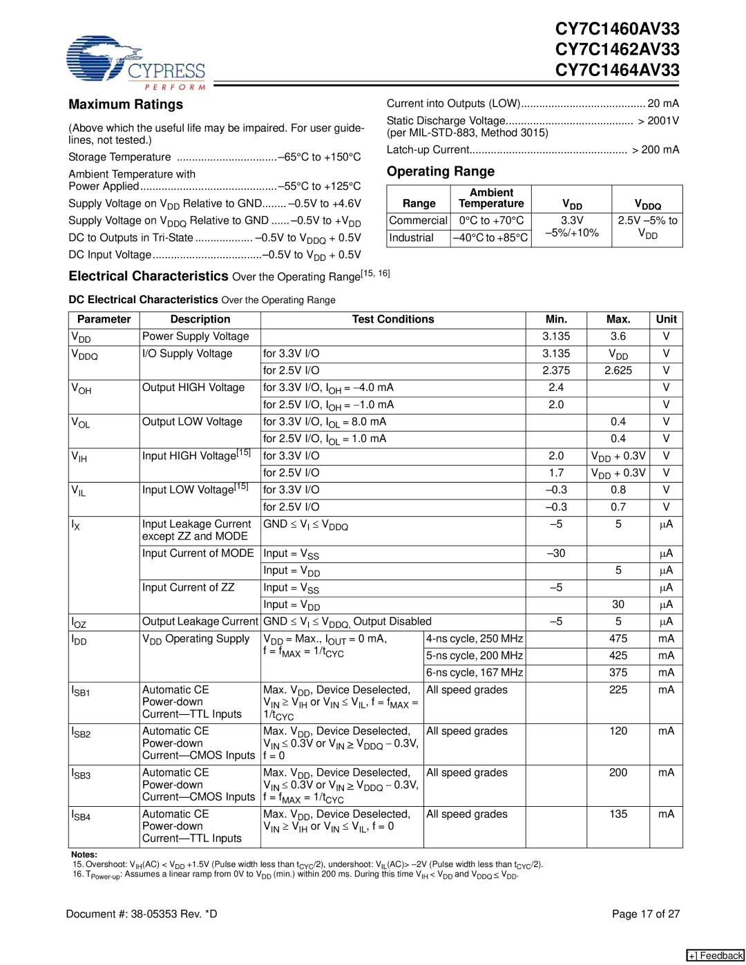
Low power consumption is another defining feature of the CY7C1460AV33, CY7C1464AV33, and CY7C1462AV33. These devices utilize advanced CMOS technology, ensuring minimal energy usage without sacrificing performance. This is particularly advantageous for battery-operated devices and applications where energy efficiency is critical.
The SRAM devices also boast robust reliability and environmental tolerance. They are designed to operate over a wide temperature range, making them suitable for various operating conditions. Additionally, the use of advanced process technology ensures data integrity and durability, allowing them to survive in harsh environments.
Furthermore, the devices support a simple interfacing design, enabling easy integration into existing systems. They feature dual-chip select and byte write functionality, which enhances flexibility in memory handling, providing the capability to manage data more effectively.
In summary, the Cypress CY7C1460AV33, CY7C1464AV33, and CY7C1462AV33 offer high-speed, low-power, and highly reliable SRAM solutions suitable for various applications. With their advanced technology and robust characteristics, these devices are invaluable in modern electronic design, enabling innovation and performance optimization across diverse fields.