CY7C1470BV33 CY7C1472BV33, CY7C1474BV33
possible to capture all other signals and simply ignore the value of the CLK captured in the boundary scan register.
After the data is captured, it is possible to shift out the data by putting the TAP into the
Note that since the PRELOAD part of the command is not imple- mented, putting the TAP to the
BYPASS
When the BYPASS instruction is loaded in the instruction register and the TAP is placed in a
Reserved
These instructions are not implemented but are reserved for future use. Do not use these instructions.
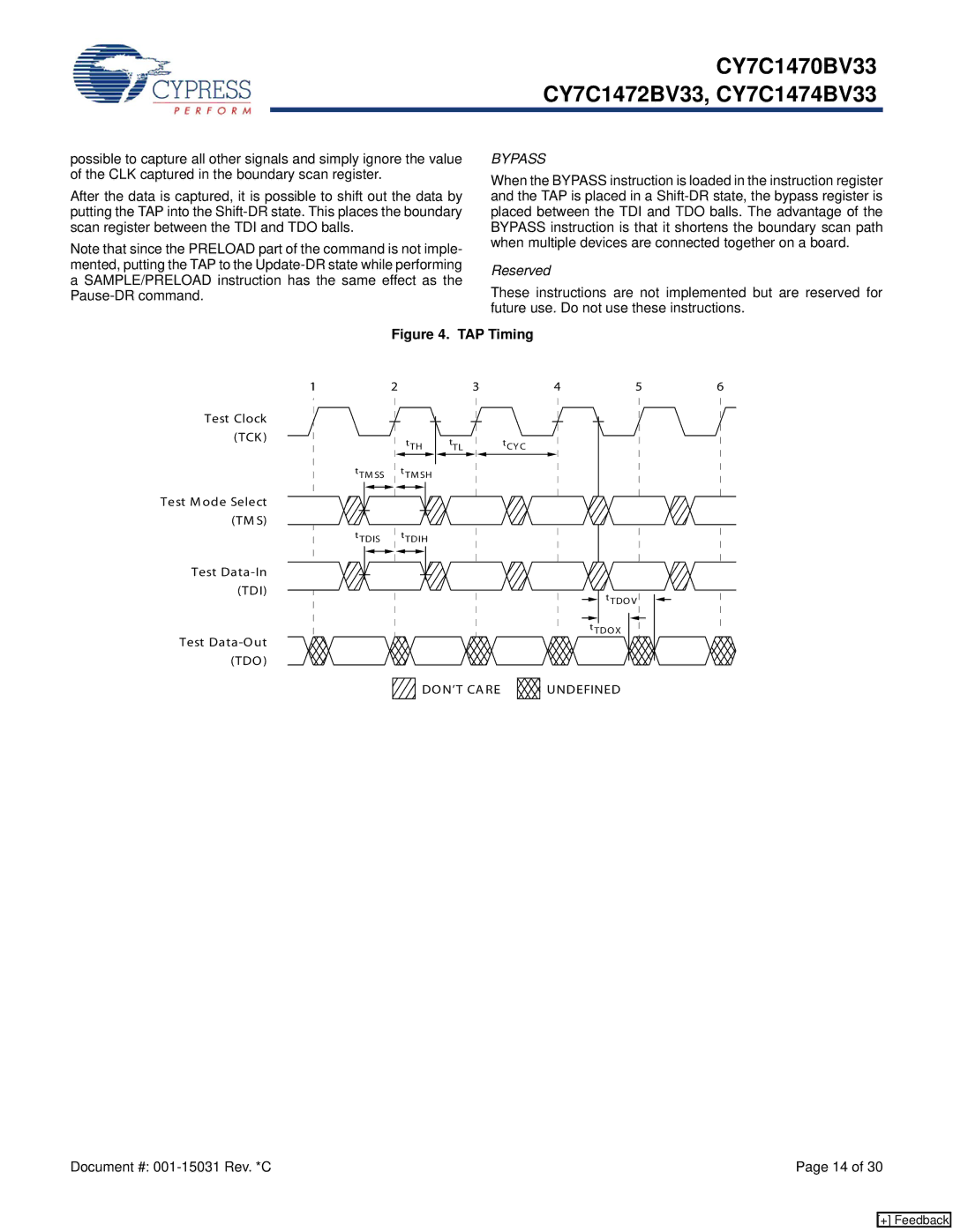
Figure 4. TAP Timing
1 |
| 2 |
|
|
|
|
|
|
Test Clock |
|
|
|
|
|
|
| |
(TCK ) |
|
| tTH |
|
| |||
|
|
|
|
| ||||
|
|
|
| |||||
tTM SS |
| tTM SH | ||||||
|
|
|
|
|
|
|
|
|
Test M ode Select (TM S)
tTDIS tTDIH
Test
Test
3 | 4 | 5 | 6 |
tTL | tCY C |
|
|
tTDOV
tTDOX ![]()
DON’T CA RE
UNDEFINED
Document #: | Page 14 of 30 |
[+] Feedback