CY7C1470BV33
CY7C1472BV33, CY7C1474BV33
Switching Waveforms
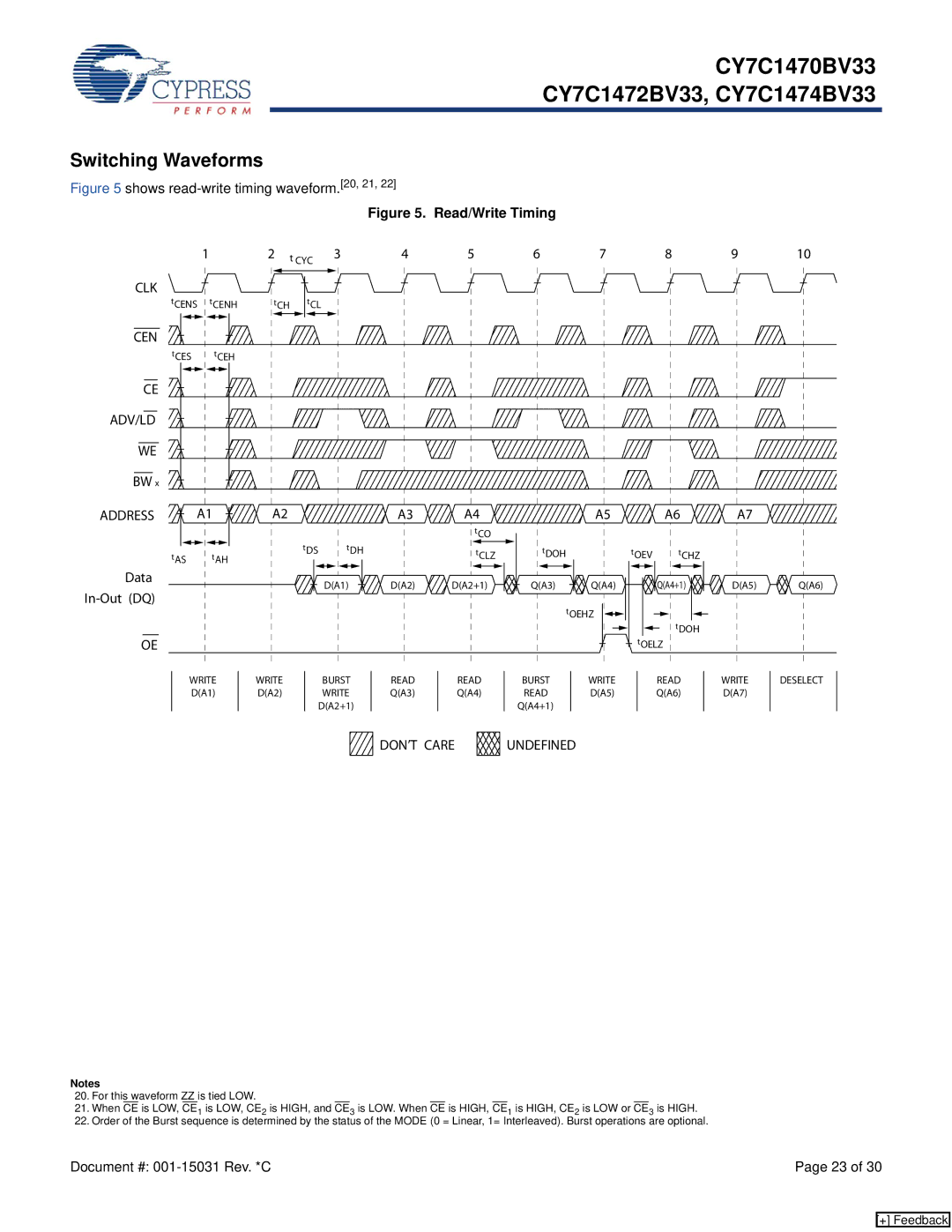
Figure 5 shows read-write timing waveform.[20, 21, 22]
Figure 5. Read/Write Timing
1 |
| 2 | t CYC | 3 | |
|
|
|
| ||
CLK |
|
|
|
|
|
tCENS | tCENH | tCH | tCL |
| |
CEN |
|
|
|
|
|
tCES | tCEH |
|
|
|
|
4 5
6 | 7 | 8 | 9 | 10 | |||||
|
|
|
|
|
|
|
|
|
|
CE |
|
ADV/LD |
|
WE |
|
BW x |
|
ADDRESS | A1 |
tAS | tAH |
Data |
|
|
A2
tDS tDH
D(A1)
A3  A4
A4
tCO
tCLZ
D(A2) ![]() D(A2+1)
D(A2+1)
| A5 |
| A6 | A7 |
|
tDOH | tOEV | tCHZ |
|
| |
Q(A3) | Q(A4) |
| Q(A4+1) | D(A5) | Q(A6) |
| tOEHZ |
|
|
|
|
|
|
| tDOH |
|
|
OE
WRITE | WRITE | BURST | |
D(A1) | D(A2) | WRITE | |
|
| D(A2+1) | |
|
|
|
|
|
|
|
|
tOELZ |
READ | READ | BURST | WRITE | READ | WRITE | DESELECT |
Q(A3) | Q(A4) | READ | D(A5) | Q(A6) | D(A7) |
|
|
| Q(A4+1) |
|
|
|
|
DON’T CARE |
| UNDEFINED |
|
|
|
|
Notes
20.For this waveform ZZ is tied LOW.
21.When CE is LOW, CE1 is LOW, CE2 is HIGH, and CE3 is LOW. When CE is HIGH, CE1 is HIGH, CE2 is LOW or CE3 is HIGH.
22.Order of the Burst sequence is determined by the status of the MODE (0 = Linear, 1= Interleaved). Burst operations are optional.
Document #: | Page 23 of 30 |
[+] Feedback