CY7C1470BV33
CY7C1472BV33, CY7C1474BV33
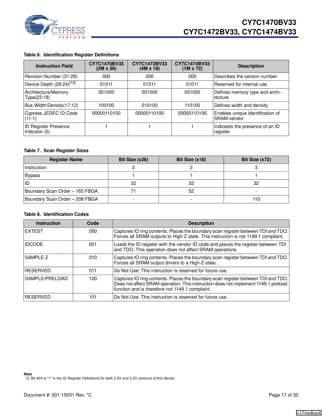
Table 6. Identification Register Definitions
Instruction Field | CY7C1470BV33 | CY7C1472BV33 | CY7C1474BV33 | Description | |
(2M x 36) | (4M x 18) | (1M x 72) | |||
|
| ||||
Revision Number (31:29) | 000 | 000 | 000 | Describes the version number | |
|
|
|
|
| |
Device Depth (28:24)[12] | 01011 | 01011 | 01011 | Reserved for internal use | |
Architecture/Memory | 001000 | 001000 | 001000 | Defines memory type and archi- | |
Type(23:18) |
|
|
| tecture | |
Bus Width/Density(17:12) | 100100 | 010100 | 110100 | Defines width and density | |
|
|
|
|
| |
Cypress JEDEC ID Code | 00000110100 | 00000110100 | 00000110100 | Enables unique identification of | |
(11:1) |
|
|
| SRAM vendor | |
ID Register Presence | 1 | 1 | 1 | Indicates the presence of an ID | |
Indicator (0) |
|
|
| register |
Table 7. Scan Register Sizes
Register Name |
|
| Bit Size (x36) | Bit Size (x18) |
| Bit Size (x72) | |
Instruction |
| 3 | 3 |
| 3 | ||
|
|
|
|
|
|
|
|
Bypass |
| 1 | 1 |
| 1 | ||
|
|
|
|
|
|
|
|
ID |
| 32 | 32 |
| 32 | ||
|
|
|
|
|
|
| |
Boundary Scan Order – 165 FBGA | 71 | 52 |
| - | |||
|
|
|
|
|
|
| |
Boundary Scan Order – 209 FBGA | - | - |
| 110 | |||
|
|
|
|
|
|
| |
Table 8. Identification Codes |
|
|
|
|
| ||
|
|
|
|
|
|
| |
Instruction |
| Code |
|
| Description |
| |
EXTEST |
| 000 |
| Captures IO ring contents. Places the boundary scan register between TDI and TDO. | |||
|
|
|
| Forces all SRAM outputs to | |||
IDCODE |
| 001 |
| Loads the ID register with the vendor ID code and places the register between TDI | |||
|
|
|
| and TDO. This operation does not affect SRAM operations. |
| ||
SAMPLE Z |
| 010 |
| Captures IO ring contents. Places the boundary scan register between TDI and TDO. | |||
|
|
|
| Forces all SRAM output drivers to a |
| ||
RESERVED |
| 011 |
| Do Not Use: This instruction is reserved for future use. |
| ||
|
|
|
|
| |||
SAMPLE/PRELOAD |
| 100 |
| Captures IO ring contents. Places the boundary scan register between TDI and TDO. | |||
|
|
|
| Does not affect SRAM operation. This instruction does not implement 1149.1 preload | |||
|
|
|
| function and is therefore not 1149.1 compliant. |
| ||
RESERVED |
| 101 |
| Do Not Use: This instruction is reserved for future use. |
| ||
|
|
|
|
|
|
|
|
Note
12. Bit #24 is “1” in the ID Register Definitions for both 2.5V and 3.3V versions of this device.
Document #: | Page 17 of 30 |
[+] Feedback