CY7C1470BV33
CY7C1472BV33, CY7C1474BV33
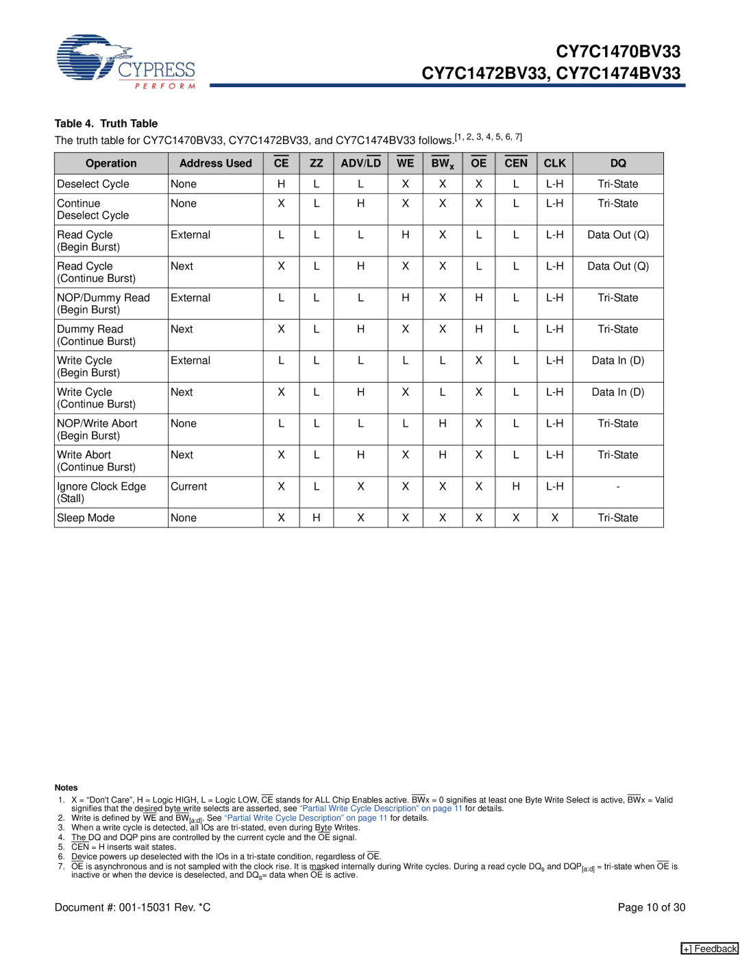
Table 4. Truth Table
The truth table for CY7C1470BV33, CY7C1472BV33, and CY7C1474BV33 follows.[1, 2, 3, 4, 5, 6, 7]
Operation | Address Used |
| CE |
| ZZ | ADV/LD |
| WE |
|
| BWx |
| OE |
|
| CEN | CLK | DQ | ||||
Deselect Cycle | None |
| H |
| L | L |
| X |
|
| X |
| X |
|
| L | ||||||
|
|
|
|
|
|
|
|
|
|
|
|
|
|
|
|
|
|
| ||||
Continue | None |
| X |
| L | H |
| X |
|
| X |
| X |
|
| L | ||||||
Deselect Cycle |
|
|
|
|
|
|
|
|
|
|
|
|
|
|
|
|
|
|
|
|
|
|
Read Cycle | External |
| L |
| L | L |
| H |
|
| X |
| L |
|
| L | Data Out (Q) | |||||
(Begin Burst) |
|
|
|
|
|
|
|
|
|
|
|
|
|
|
|
|
|
|
|
|
|
|
Read Cycle | Next |
| X |
| L | H |
| X |
|
| X |
| L |
|
| L | Data Out (Q) | |||||
(Continue Burst) |
|
|
|
|
|
|
|
|
|
|
|
|
|
|
|
|
|
|
|
|
|
|
NOP/Dummy Read | External |
| L |
| L | L |
| H |
|
| X |
| H |
|
| L | ||||||
(Begin Burst) |
|
|
|
|
|
|
|
|
|
|
|
|
|
|
|
|
|
|
|
|
|
|
Dummy Read | Next |
| X |
| L | H |
| X |
|
| X |
| H |
|
| L | ||||||
(Continue Burst) |
|
|
|
|
|
|
|
|
|
|
|
|
|
|
|
|
|
|
|
|
|
|
Write Cycle | External |
| L |
| L | L |
| L |
|
| L |
| X |
|
| L | Data In (D) | |||||
(Begin Burst) |
|
|
|
|
|
|
|
|
|
|
|
|
|
|
|
|
|
|
|
|
|
|
Write Cycle | Next |
| X |
| L | H |
| X |
|
| L |
| X |
|
| L | Data In (D) | |||||
(Continue Burst) |
|
|
|
|
|
|
|
|
|
|
|
|
|
|
|
|
|
|
|
|
|
|
NOP/Write Abort | None |
| L |
| L | L |
| L |
|
| H |
| X |
|
| L | ||||||
(Begin Burst) |
|
|
|
|
|
|
|
|
|
|
|
|
|
|
|
|
|
|
|
|
|
|
Write Abort | Next |
| X |
| L | H |
| X |
|
| H |
| X |
|
| L | ||||||
(Continue Burst) |
|
|
|
|
|
|
|
|
|
|
|
|
|
|
|
|
|
|
|
|
|
|
Ignore Clock Edge | Current |
| X |
| L | X |
| X |
|
| X |
| X |
|
| H | - | |||||
(Stall) |
|
|
|
|
|
|
|
|
|
|
|
|
|
|
|
|
|
|
|
|
|
|
Sleep Mode | None |
| X |
| H | X |
| X |
|
| X |
| X |
|
| X | X | |||||
|
|
|
|
|
|
|
|
|
|
|
|
|
|
|
|
|
|
|
|
|
|
|
Notes
1.X = “Don't Care”, H = Logic HIGH, L = Logic LOW, CE stands for ALL Chip Enables active. BWx = 0 signifies at least one Byte Write Select is active, BWx = Valid signifies that the desired byte write selects are asserted, see “Partial Write Cycle Description” on page 11 for details.
2.Write is defined by WE and BW[a:d]. See “Partial Write Cycle Description” on page 11 for details.
3.When a write cycle is detected, all IOs are
4.The DQ and DQP pins are controlled by the current cycle and the OE signal.
5.CEN = H inserts wait states.
6.Device powers up deselected with the IOs in a
7.OE is asynchronous and is not sampled with the clock rise. It is masked internally during Write cycles. During a read cycle DQs and DQP[a:d] =
Document #: | Page 10 of 30 |
[+] Feedback