|
| PRELIMINARY | CY7C2561KV18, CY7C2576KV18 | |
|
| CY7C2563KV18, CY7C2565KV18 | ||
|
|
| ||
|
|
|
|
|
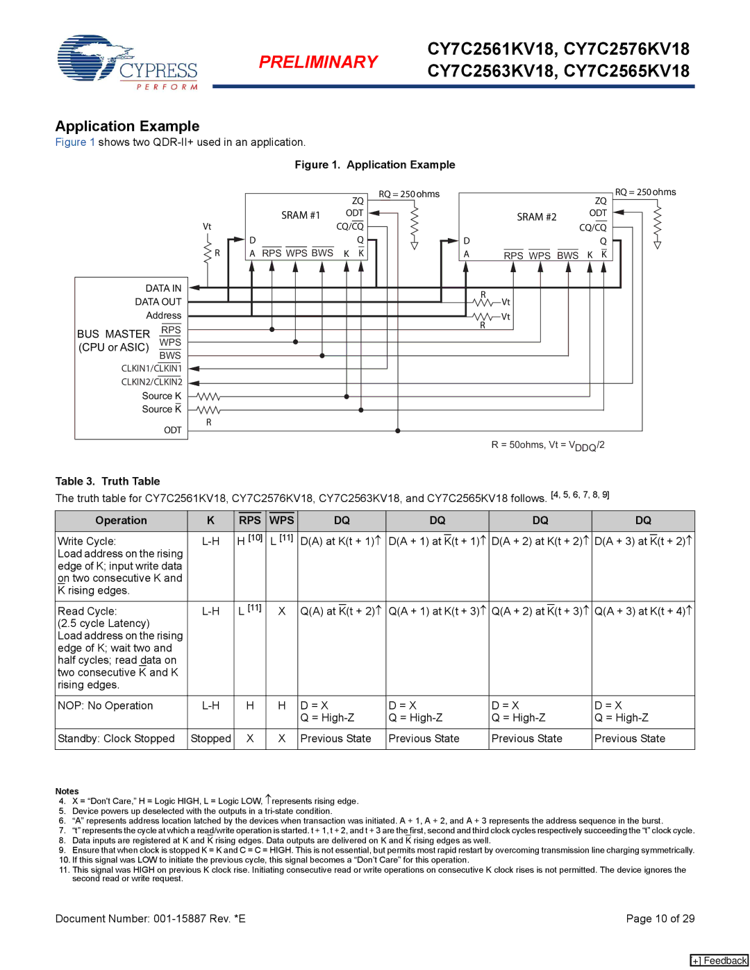
Application Example
Figure 1 shows two QDR-II+ used in an application.
Figure 1. Application Example
DATA IN
DATA OUT
Address
BUS MASTER RPS
(CPU or ASIC) WPS BWS
CLKIN1/CLKIN1
CLKIN2/CLKIN2
Source K
Source K
ODT
|
|
| ZQ | RQ = 250 ohms |
| RQ = 250 ohms |
|
|
|
|
| ZQ | |
|
| SRAM #1 | ODT |
| SRAM #2 | ODT |
Vt |
|
| CQ/CQ |
|
| CQ/CQ |
| D | RPS WPS BWS | Q | D |
| Q |
R | A | K K | A | RPS WPS BWS | K K | |
|
|
|
|
| R |
|
|
|
|
|
| Vt |
|
|
|
|
|
| Vt |
|
|
|
|
|
| R |
|
R |
|
|
|
|
|
|
|
|
|
|
| R = 50ohms, Vt = VDDQ/2 | |
Table 3. Truth Table
The truth table for CY7C2561KV18, CY7C2576KV18, CY7C2563KV18, and CY7C2565KV18 follows. [4, 5, 6, 7, 8, 9]
Operation | K | RPS | WPS | DQ | DQ | DQ | DQ | ||||||||
Write Cycle: | H [10] | L [11] | D(A) at K(t + 1)↑ | D(A + 1) at |
|
| D(A + 2) at K(t + 2)↑ |
|
|
| |||||
K(t + 1)↑ | D(A + 3) at K(t + 2)↑ | ||||||||||||||
Load address on the rising |
|
|
|
|
|
|
|
|
|
|
|
|
|
|
|
edge of K; input write data |
|
|
|
|
|
|
|
|
|
|
|
|
|
|
|
on two consecutive K and |
|
|
|
|
|
|
|
|
|
|
|
|
|
|
|
K rising edges. |
|
|
|
|
|
|
|
|
|
|
|
|
|
|
|
|
|
|
|
|
|
|
|
|
|
| |||||
Read Cycle: | L [11] | X | Q(A) at |
|
| Q(A + 1) at K(t + 3)↑ |
|
|
| Q(A + 3) at K(t + 4)↑ | |||||
K(t + 2)↑ | Q(A + 2) at K(t + 3)↑ | ||||||||||||||
(2.5 cycle Latency) |
|
|
|
|
|
|
|
|
|
|
|
|
|
|
|
Load address on the rising |
|
|
|
|
|
|
|
|
|
|
|
|
|
|
|
edge of K; wait two and |
|
|
|
|
|
|
|
|
|
|
|
|
|
|
|
half cycles; read data on |
|
|
|
|
|
|
|
|
|
|
|
|
|
|
|
two consecutive K and K |
|
|
|
|
|
|
|
|
|
|
|
|
|
|
|
rising edges. |
|
|
|
|
|
|
|
|
|
|
|
|
|
|
|
|
|
|
|
|
|
|
| ||||||||
NOP: No Operation | H | H | D = X | D = X | D = X | D = X | |||||||||
|
|
|
| Q = | Q = | Q = | Q = | ||||||||
|
|
|
|
|
|
|
| ||||||||
Standby: Clock Stopped | Stopped | X | X | Previous State | Previous State | Previous State | Previous State | ||||||||
|
|
|
|
|
|
|
|
|
|
|
|
|
|
|
|
Notes
4.X = “Don't Care,” H = Logic HIGH, L = Logic LOW, ↑represents rising edge.
5.Device powers up deselected with the outputs in a
6.“A” represents address location latched by the devices when transaction was initiated. A + 1, A + 2, and A + 3 represents the address sequence in the burst.
7.“t” represents the cycle at which a read/write operation is started. t + 1, t + 2, and t + 3 are the first, second and third clock cycles respectively succeeding the “t” clock cycle.
8.Data inputs are registered at K and K rising edges. Data outputs are delivered on K and K rising edges as well.
9.Ensure that when clock is stopped K = K and C = C = HIGH. This is not essential, but permits most rapid restart by overcoming transmission line charging symmetrically.
10.If this signal was LOW to initiate the previous cycle, this signal becomes a “Don’t Care” for this operation.
11.This signal was HIGH on previous K clock rise. Initiating consecutive read or write operations on consecutive K clock rises is not permitted. The device ignores the second read or write request.
Document Number: | Page 10 of 29 |
[+] Feedback