CY8C24223A, CY8C24423A
DC Analog PSoC Block Specifications
The following table lists guaranteed maximum and minimum specifications for the voltage and temperature ranges: 4.75V to 5.25V and
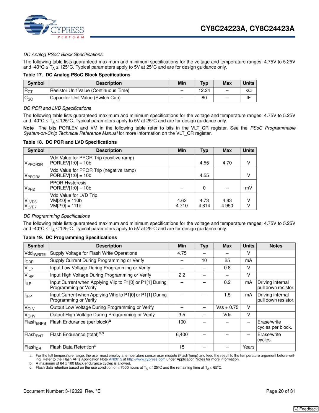
Table 17. DC Analog PSoC Block Specifications
Symbol | Description | Min | Typ | Max | Units |
RCT | Resistor Unit Value (Continuous Time) | – | 12.24 | – | kΩ |
CSC | Capacitor Unit Value (Switch Cap) | – | 80 | – | fF |
DC POR and LVD Specifications
The following table lists guaranteed maximum and minimum specifications for the voltage and temperature ranges: 4.75V to 5.25V and
Note The bits PORLEV and VM in the following table refer to bits in the VLT_CR register. See the PSoC Programmable
Table 18. DC POR and LVD Specifications
Symbol | Description | Min | Typ | Max | Units |
| Vdd Value for PPOR Trip (positive ramp) |
|
|
|
|
VPPOR2R | PORLEV[1:0] = 10b |
| 4.55 | 4.70 | V |
| Vdd Value for PPOR Trip (negative ramp) |
|
|
|
|
VPPOR2 | PORLEV[1:0] = 10b |
| 4.55 |
| V |
| PPOR Hysteresis |
|
|
|
|
VPH2 | PORLEV[1:0] = 10b | – | 0 | – | mV |
| Vdd Value for LVD Trip |
|
|
|
|
VLVD6 | VM[2:0] = 110b | 4.62 | 4.73 | 4.83 | V |
VLVD7 | VM[2:0] = 111b | 4.710 | 4.814 | 4.950 | V |
DC Programming Specifications
The following table lists guaranteed maximum and minimum specifications for the voltage and temperature ranges: 4.75V to 5.25V and
Table 19. DC Programming Specifications
Symbol | Description | Min | Typ | Max | Units | Notes |
VddIWRITE | Supply Voltage for Flash Write Operations | 4.75 | – | – | V |
|
IDDP | Supply Current During Programming or Verify | – | 10 | 25 | mA |
|
VILP | Input Low Voltage During Programming or Verify | – | – | 0.8 | V |
|
VIHP | Input High Voltage During Programming or Verify | 2.2 | – | – | V |
|
IILP | Input Current when Applying Vilp to P1[0] or P1[1] During | – | – | 0.2 | mA | Driving internal |
| Programming or Verify |
|
|
|
| pull down resistor. |
IIHP | Input Current when Applying Vihp to P1[0] or P1[1] During | – | – | 1.5 | mA | Driving internal |
| Programming or Verify |
|
|
|
| pull down resistor. |
VOLV | Output Low Voltage During Programming or Verify | – | – | Vss + 0.75 | V |
|
VOHV | Output High Voltage During Programming or Verify | 3.5 | – | Vdd | V |
|
FlashENPB | Flash Endurance (per block)a | 100 | – | – | – | Erase/write |
|
|
|
|
|
| cycles per block. |
Flash | Flash Endurance (total)a,b | 6,400 | – | – | – | Erase/write |
ENT |
|
|
|
|
| cycles. |
|
|
|
|
|
| |
|
|
|
|
|
|
|
Flash | Flash Data Retentionc | 15 | – | – | Years |
|
DR |
|
|
|
|
|
|
a.For the full temperature range, the user must employ a temperature sensor user module (FlashTemp) and feed the result to the temperature argument before writ- ing. Refer to the Flash APIs Application Note AN2015 at http://www.cypress.com under Application Notes for more information.
b.A maximum of 64 x 100 block endurance cycles is allowed.
c.Flash data retention based on the use condition of ≤ 7000 hours at TA ≤ 125°C and the remaining time at TA ≤ 65°C.
Document Number: | Page 20 of 31 |
[+] Feedback
