Manuals
/
Brands
/
Computer Equipment
/
Computer Hardware
/
Cypress
/
Computer Equipment
/
Computer Hardware
Cypress
STK11C68-5
Package Diagrams
1
14
15
15
Download
15 pages, 531.03 Kb
STK11C68-5 (SMD5962-92324)
Document Number: 001-51001 Rev. *A
Page 14 of 15
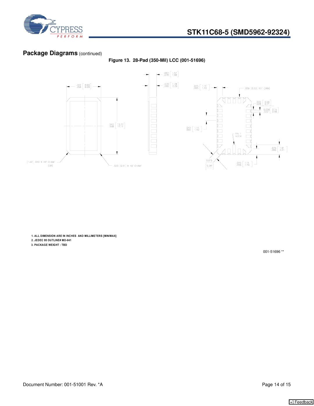
Figure 13. 28-Pad (350-Mil) LCC (001-51696)
Package Diagrams
(continued)
1.ALL D IMENSION A RE IN INCHES AND MILLIMETER S [MIN/MAX]
2.JEDEC 95 OUTLINE# M O-041
3.PACKAGE WEIGHT : TBD
001-51696 **
[+] Feedback
Contents
Main
STK11C68-5 (SMD5962-92324)
64 Kbit (8K x 8) SoftStore nvSRAM
Features
Functional Description
Logic Block Diagram
STK11C68-5 (SMD5962-92324)
Pinouts
Figure 1. Pin Diagram - 28-Pin DIP
Pin Definitions
Figure 2. Pin Diagram - 28-Pin LLC
STK11C68-5 (SMD5962-92324)
Device Operation
SRAM Read
SRAM Write
Software STORE
STK11C68-5 (SMD5962-92324)
Low Average Active Power
Best Practices
STK11C68-5 (SMD5962-92324)
Maximum Ratings
Operating Range
DC Electrical Characteristics
Data Retention and Endurance
STK11C68-5 (SMD5962-92324)
Thermal Resistance
AC Test Conditions
AC Switching Characteristics
SRAM Read Cycle
Switching Waveforms
STK11C68-5 (SMD5962-92324)
Figure 9. SRAM Write Cycle 2: CE and OE Controlled [7, 8]
[+] Feedback
SRAM Write Cycle
Parameter Description 35 ns 45 ns 55 ns Unit Min Max Min Max Min Max
STK11C68-5 (SMD5962-92324)
AutoStore INHIBIT or Power Up RECALL
[+] Feedback
Software Controlled STORE/RECALL Cycle
Switching Waveform
/ t
STK11C68-5 (SMD5962-92324)
Part Numbering Nomenclature STK11C68 - 5 C 45 M
SMD5962-92324 04 MX X
Ordering Information
Page
Package Diagrams
Document History Page
Sales, Solutions, and Legal Information
Worldwide Sales and Design Support
Products
PSoC Solutions