DLL Timing Control Registers, RCOMP settings
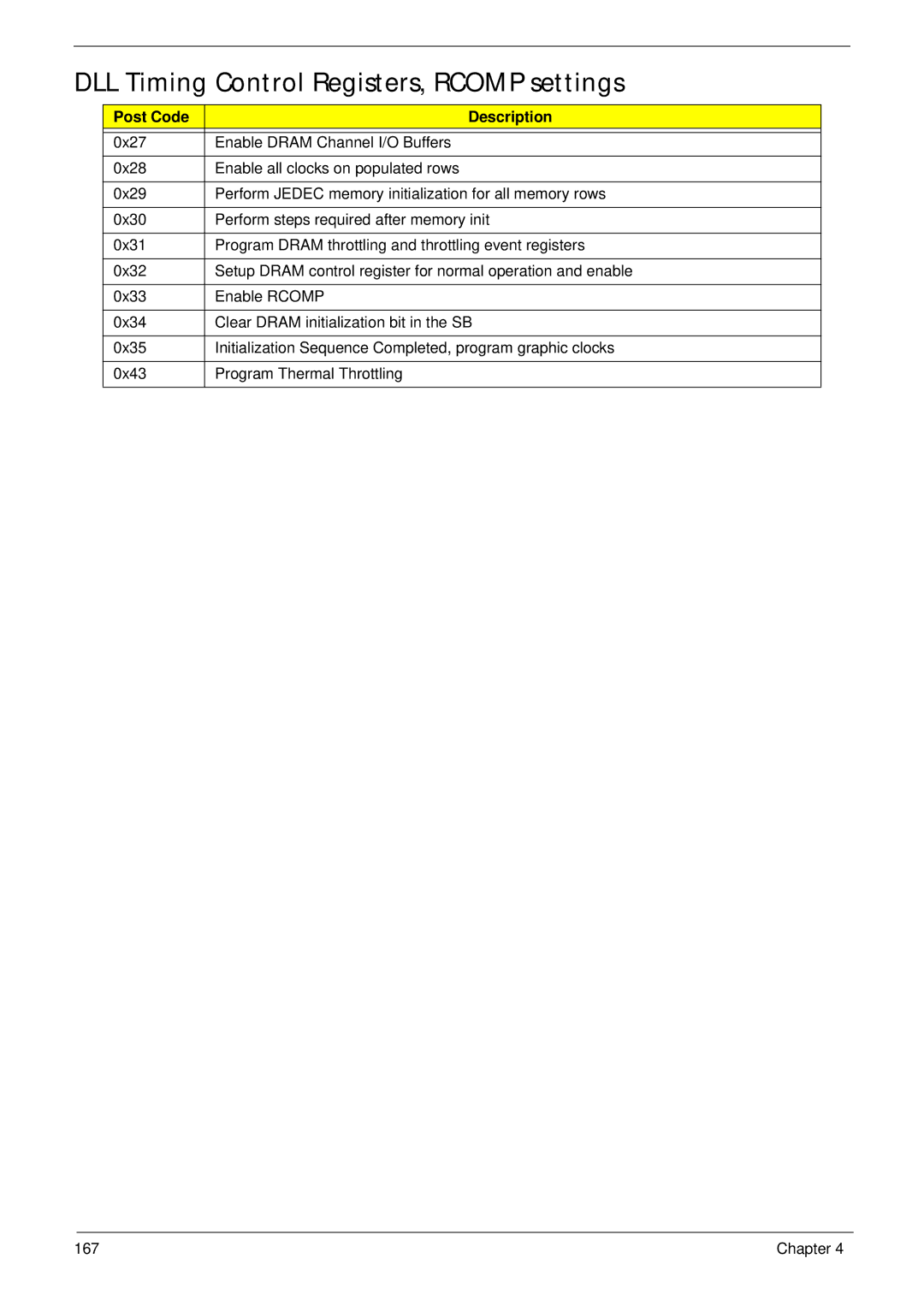
Post Code | Description |
|
|
0x27 | Enable DRAM Channel I/O Buffers |
0x28 | Enable all clocks on populated rows |
|
|
0x29 | Perform JEDEC memory initialization for all memory rows |
|
|
0x30 | Perform steps required after memory init |
|
|
0x31 | Program DRAM throttling and throttling event registers |
|
|
0x32 | Setup DRAM control register for normal operation and enable |
|
|
0x33 | Enable RCOMP |
|
|
0x34 | Clear DRAM initialization bit in the SB |
|
|
0x35 | Initialization Sequence Completed, program graphic clocks |
|
|
0x43 | Program Thermal Throttling |
|
|
167 | Chapter 4 |
