Application Note 7502
100 |
|
|
|
| |
| 75 |
|
|
|
|
DSS |
|
|
|
|
|
V | 50 |
|
|
|
|
RATES |
|
|
|
| |
| RFM15N15 |
|
| ||
| IT = 1mA |
|
| ||
% |
| VG = 10 VOLTS |
|
| |
| 25 | RL = VDSS/ID(RMS) |
|
| |
| 0 |
|
|
|
|
|
| 20IT/IG | 40IT/IG | 60IT/IG | 80IT/IG |
TIME - microseconds
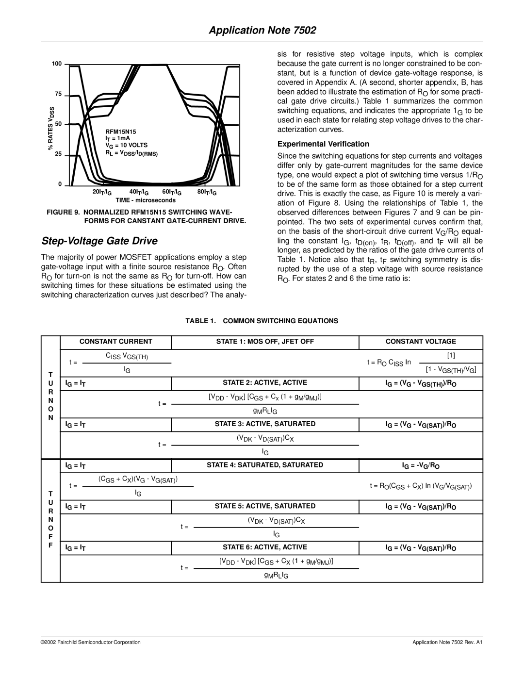
FIGURE 9. NORMALIZED RFM15N15 SWITCHING WAVE- FORMS FOR CANSTANT GATE-CURRENT DRIVE.
Step-Voltage Gate Drive
The majority of power MOSFET applications employ a step
sis for resistive step voltage inputs, which is complex because the gate current is no longer constrained to be con- stant, but is a function of device
Experimental Verification
Since the switching equations for step currents and voltages differ only by
ling the constant IG, tD(on), tR, tD(off), and tF will all be longer, as predicted by the ratios of the gate drive currents of
Table 1. Notice also that tR, tF switching symmetry is dis- rupted by the use of a step voltage with source resistance RO. For states 2 and 6 the time ratio is:
TABLE 1. COMMON SWITCHING EQUATIONS
|
| CONSTANT CURRENT |
|
| STATE 1: MOS OFF, JFET OFF | CONSTANT VOLTAGE | ||
|
|
|
|
|
|
|
|
|
|
| t = | CISS VGS(TH) |
|
| [1] | ||
|
|
|
|
|
| t = RO CISS In |
| |
T |
| IG |
|
| [1 - VGS(TH)/VG] | |||
|
|
|
|
| ||||
U | IG = IT |
|
| STATE 2: ACTIVE, ACTIVE | IG = (VG - VGS(TH))/RO | |||
R |
|
|
|
|
|
|
|
|
|
|
|
|
| [VDD - VDK] [CGS + Cx (1 + gM/gMJ)] |
|
| |
N |
| t = |
|
|
|
| ||
O |
|
|
| gMRLIG |
|
| ||
|
|
|
|
|
| |||
N |
|
|
|
|
|
|
|
|
| IG = IT |
|
| STATE 3: ACTIVE, SATURATED | IG = (VG - VG(SAT))/RO | |||
|
|
|
| |||||
|
|
| t = |
|
| (VDK - VD(SAT))CX |
|
|
|
|
|
|
| IG |
|
| |
|
|
|
|
|
|
|
| |
|
| IG = IT |
|
| STATE 4: SATURATED, SATURATED | IG = | ||
|
| t = | (CGS + CX)(VG - VG(SAT)) |
|
| t = RO(CGS + CX) In (VG/VG(SAT)) | ||
T | IG |
|
| |||||
|
|
|
|
| ||||
U |
| IG = IT |
|
| STATE 5: ACTIVE, SATURATED | IG = (VG - VG(SAT))/RO | ||
R |
|
|
| |||||
N |
|
|
| t = | (VDK - VD(SAT))CX |
|
| |
O |
|
|
|
|
|
| ||
|
|
| IG |
|
| |||
F |
|
|
|
|
|
| ||
F |
| IG = IT |
|
| STATE 6: ACTIVE, ACTIVE | IG = (VG - VG(SAT))/RO | ||
|
|
|
|
| t = | [VDD - VDK] [CGS + CX (1 + gM/gMJ)] |
|
|
|
|
|
|
| gMRLIG |
|
| |
|
|
|
|
|
|
|
| |
©2002 Fairchild Semiconductor Corporation | Application Note 7502 Rev. A1 |