Application Note 7502
State 2: MOS ActIve, JFET ActIve
This state graphically illustrates the dramatic influence that the JFET has on the power MOSFET
dVG/dt = gMRLlG/[CGS + CX(1 + gM/gMJ)]
In all but the smallest
CRSS (CRSS = CGD) is a small value, as
CRSS were, in actuality, small, long drain voltage tails would not exist. The tail response is a direct result of JFET satura- tion. In order to delineate the transition from state 2 to state 3, a drain voltage at which the transition occurs must be defined. VDK is the knee voltage at which linear extrapola- tions of
t2(t6) = (VDD - VDK)[CGS + CX(1 + gM/gMJ)]/gMRLIG
State 3: MOS Active, JFET Saturated
When the JFET saturates, the gMJVX current generator becomes a short circuit and the equivalent circuit predicts:
dVD/dt = gMRLIG/[CGS + CX(1 + gMRL)]
This is the Miller effect so often referred to in older texts that describe the behavior of
t3(t5) = (VDK - VD(SAT))Cx/lG
State 4: MOS Saturated, JFET Saturated (Turn-Off)
In this state, in addition to gMJVX being shorted, the gMVG cur- rent generator is shorted, and IG is occupied with charging CX
and CGS, in parallel, from the peak value of VG to VG(SAT). The time required for this is:
t4 = (VG - VG(SAT))(CGS + Cx)/IG
Since a value for CGS may be measured independently of switching time, the method described is the simplest way of determining CX.
On
Experimental Verification
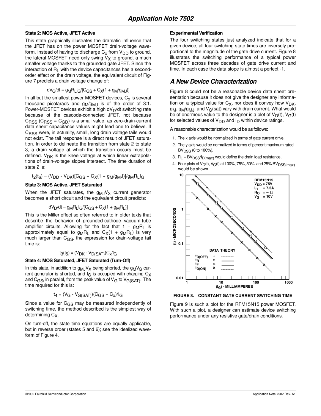
The four switching states just analyzed indicate that for a given device, all four switching state times are inversely pro- portional to the magnitude of the gate drive current. Figure 8 illustrates the switching performance of a typical power MOSFET across three decades of gate drive current and time. In each case the data slope is almost a perfect
A New Device Characterization
Figure 8 could not be a reasonable device data sheet pre- sentation because it does not give the designer any informa- tion on a typical value for CX, nor does it convey how VDK, gM, gM/gMJ, and VG(sat) vary with drain current. What would be of enormous value to the designer is a plot of VD(t), VG(t) for selected values of VDD and ID within device ratings.
A reasonable characterization would be as follows:
1.The x axis would be normalized in terms of gate current drive.
2.The y axis would be normalized in terms of percent maximum rated BVDSS (0 to 100%).
3.RL = BVDSS/ID(max) would define the drain load resistance.
4.Four plots of VD(t), VG(t) at 100%, 75%, 50%, and 25% BVDSS(max) would be shown.
| 10 |
|
|
|
|
|
| RFM15N15 | |
|
|
| VDD = 75V | |
|
|
| ID | = 7.5A |
|
|
| RO | = ∞ Ω |
|
|
| VG | = 10V |
(t) - MICROSECONDS | 1 |
|
|
|
0.1 |
|
|
| |
|
| DATA THEORY |
|
|
|
| tD(OFF) |
|
|
|
| tR |
|
|
|
| tF |
|
|
|
| tD(ON) |
|
|
| 0.01 |
|
|
|
| 1 | 10 | 100 | 1000 |
|
| (IG) - MILLIAMPERES |
|
|
FIGURE 8. CONSTANT GATE CURRENT SWITCHING TIME
Figure 9 is such a plot for the RFM15N15 power MOSFET. With such a plot, a designer can estimate device switching performance under any resistive gate/drain conditions
©2002 Fairchild Semiconductor Corporation | Application Note 7502 Rev. A1 |