Application Note 7502
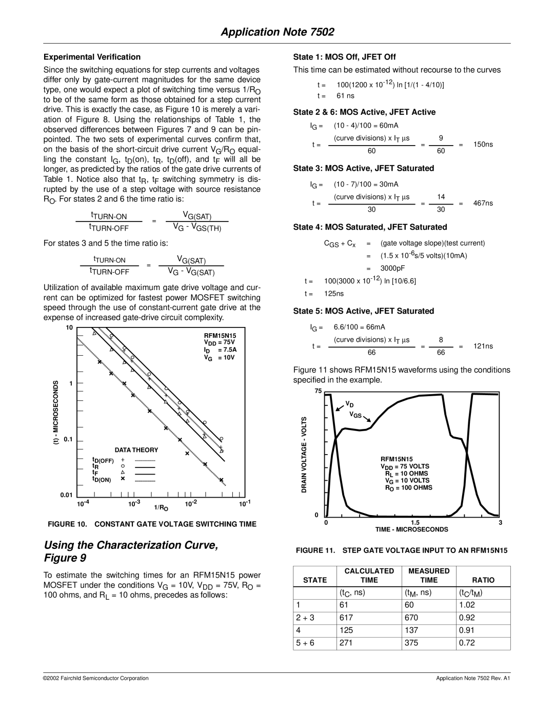
Experimental Verification
Since the switching equations for step currents and voltages differ only by
= | VG(SAT) |
For states 3 and 5 the time ratio is:
| V | ||
| = | G(SAT) | |
VG - V | |||
|
Utilization of available maximum gate drive voltage and cur- rent can be optimized for fastest power MOSFET switching speed through the use of
| 10 |
|
|
|
|
|
| RFM15N15 | |
|
|
| VDD = 75V | |
|
|
| ID | = 7.5A |
|
|
| VG | = 10V |
- MICROSECONDS | 1 |
|
|
|
0.1 |
|
|
| |
(t) |
|
|
| |
|
|
|
| |
|
| DATA THEORY |
|
|
|
| tD(OFF) |
|
|
|
| tR |
|
|
|
| tF |
|
|
|
| tD(ON) |
|
|
| 0.01 |
|
|
|
| ||||
|
| 1/RO |
|
|
FIGURE 10. CONSTANT GATE VOLTAGE SWITCHING TIME
Using the Characterization Curve, Figure 9
To estimate the switching times for an RFM15N15 power MOSFET under the conditions VG = 10V, VDD = 75V, RO =
100 ohms, and RL = 10 ohms, precedes as follows:
State 1: MOS Off, JFET Off
This time can be estimated without recourse to the curves
t = 100(1200 x
t = 61 ns
State 2 & 6: MOS Active, JFET Active
IG = (10 - 4)/100 = 60mA |
|
|
| |
t = | (curve divisions) x IT ∝s | = | 9 | = 150ns |
60 |
| 60 |
| |
State 3: MOS Active, JFET Saturated
IG = (10 - 7)/100 = 30mA |
|
|
| |
t = | (curve divisions) x IT ∝s | = | 14 | = 467ns |
30 |
| 30 |
| |
State 4: MOS Saturated, JFET Saturated
CGS + Cx = (gate voltage slope)(test current)
=(1.5 x
=3000pF
t = 100(3000 x
State 5: MOS Active, JFET Saturated
IG = 6.6/100 = 66mA |
|
|
| |
t = | (curve divisions) x IT ∝s | = | 8 | = 121ns |
66 |
| 66 |
| |
Figure 11 shows RFM15N15 waveforms using the conditions specified in the example.
75 |
|
|
| VD |
|
- VOLTS | VGS |
|
|
| |
VOLTAGE | RFM15N15 |
|
VDD = 75 VOLTS |
| |
DRAIN | RL = 10 OHMS |
|
VG = 10 VOLTS |
| |
RO = 100 OHMS |
| |
0 |
|
|
0 | 1.5 | 3 |
| TIME - MICROSECONDS |
|
FIGURE 11. STEP GATE VOLTAGE INPUT TO AN RFM15N15
| CALCULATED | MEASURED |
|
STATE | TIME | TIME | RATIO |
|
|
|
|
| (tC, ns) | (tM, ns) | (tC/tM) |
1 | 61 | 60 | 1.02 |
|
|
|
|
2 + 3 | 617 | 670 | 0.92 |
|
|
|
|
4 | 125 | 137 | 0.91 |
|
|
|
|
5 + 6 | 271 | 375 | 0.72 |
|
|
|
|
©2002 Fairchild Semiconductor Corporation | Application Note 7502 Rev. A1 |