Application Note 7502
For peak gate voltages other than 10 volts, and load resis-
tances other than BVDSS/ID(MAX), the equations of Table 1 may be used in conjunction with slope estimates from the
characterization curves for CX and CGS + CX(1 + gM/gMJ) at the appropriate
Characterization-Curve Limits
The
| 104 |
|
|
|
|
|
|
|
|
|
|
|
| RFM15N15 |
|
|
|
|
|
|
| tD(OFF) |
|
| 103 |
|
|
|
| tR |
|
|
|
|
|
| tF |
| |
|
|
|
|
|
| tD(ON) |
|
- MICROSECONDS | 102 |
|
|
|
|
|
|
101 |
|
|
|
|
|
| |
|
|
|
|
|
|
| |
TIME(t) | 100 |
|
|
|
|
|
|
|
|
|
|
|
|
| |
|
|
|
|
|
|
| |
|
|
|
|
|
|
| |
| 100 | 101 | 102 | 103 | 104 | 105 | 106 |
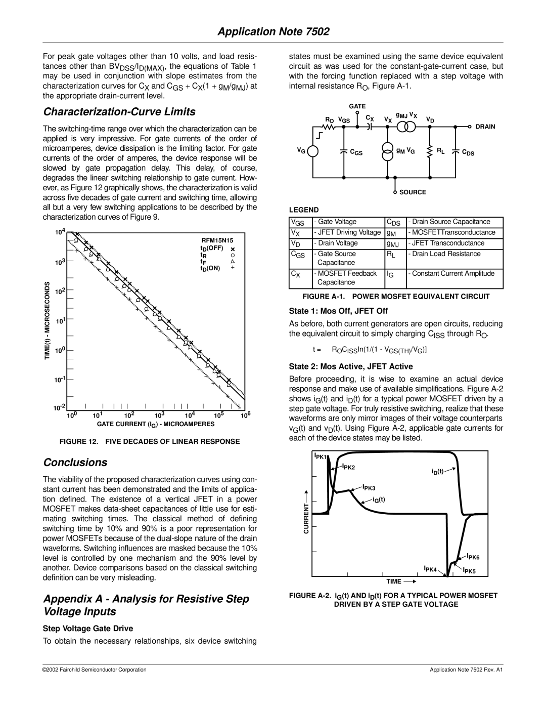
GATE CURRENT (IG) - MICROAMPERES
FIGURE 12. FIVE DECADES OF LINEAR RESPONSE
Conclusions
The viability of the proposed characterization curves using con- stant current has been demonstrated and the limits of applica- tion defined. The existence of a vertical JFET in a power MOSFET makes
Appendix A - Analysis for Resistive Step Voltage Inputs
Step Voltage Gate Drive
To obtain the necessary relationships, six device switching
states must be examined using the same device equivalent circuit as was used for the
| GATE |
|
|
|
|
|
|
R | V | CX | V | gMJ VX | V | D |
|
O | GS |
|
| X |
| DRAIN | |
|
|
|
|
|
|
| |
VG | CGS |
|
| gM VG |
| RL | CDS |
![]() SOURCE
SOURCE
LEGEND
VGS | - Gate Voltage | CDS | - Drain Source Capacitance |
VX | - JFET Driving Voltage | gM | - MOSFETTransconductance |
VD | - Drain Voltage | gMJ | - JFET Transconductance |
CGS | - Gate Source | RL | - Drain Load Resistance |
| Capacitance |
|
|
|
|
|
|
CX | - MOSFET Feedback | IG | - Constant Current Amplitude |
| Capacitance |
|
|
|
|
|
|
FIGURE A-1. POWER MOSFET EQUIVALENT CIRCUIT
State 1: Mos Off, JFET Off
As before, both current generators are open circuits, reducing the equivalent circuit to simply charging CISS through RO.
t = ROCISSIn(1/(1 - VGS(TH)/VG)]
State 2: Mos Active, JFET Active
Before proceeding, it is wise to examine an actual device response and make use of available simplifications. Figure
IPK1 |
|
|
IPK2 | iD(t) |
|
|
| |
| IPK3 |
|
CURRENT | iG(t) |
|
|
| |
|
| IPK6 |
| IPK4 | I |
|
| PK5 |
TIME ![]()
![]()
FIGURE A-2. iG(t) AND iD(t) FOR A TYPICAL POWER MOSFET
DRIVEN BY A STEP GATE VOLTAGE
©2002 Fairchild Semiconductor Corporation | Application Note 7502 Rev. A1 |