Application Note 7502
|
| VDD | VGS | GATE VOLTAGE | ||
|
|
| DRAIN | |||
|
|
|
| VG(SAT) | VOLTAGE | |
|
|
|
|
|
| |
VOLTAGE | 1 | 2 | 3 | 4 | 5 | 6 |
|
|
| STATES |
|
| |
|
|
|
|
|
| |
|
|
|
| IG = CONSTANT |
|
|
|
| VT |
|
|
|
|
|
|
| VDK | VD(SAT) |
|
|
IGi(t)
TURN ON
v(t) = IGt
C
i(t) = IG, 0 < t < T
TURN OFF
v(t) =
C
i(t) = IG, T < t < 2T
v(t)
v(t)
![]() C
C
i(t)
IGT
T | T | t |
IG
t
TIME ![]()
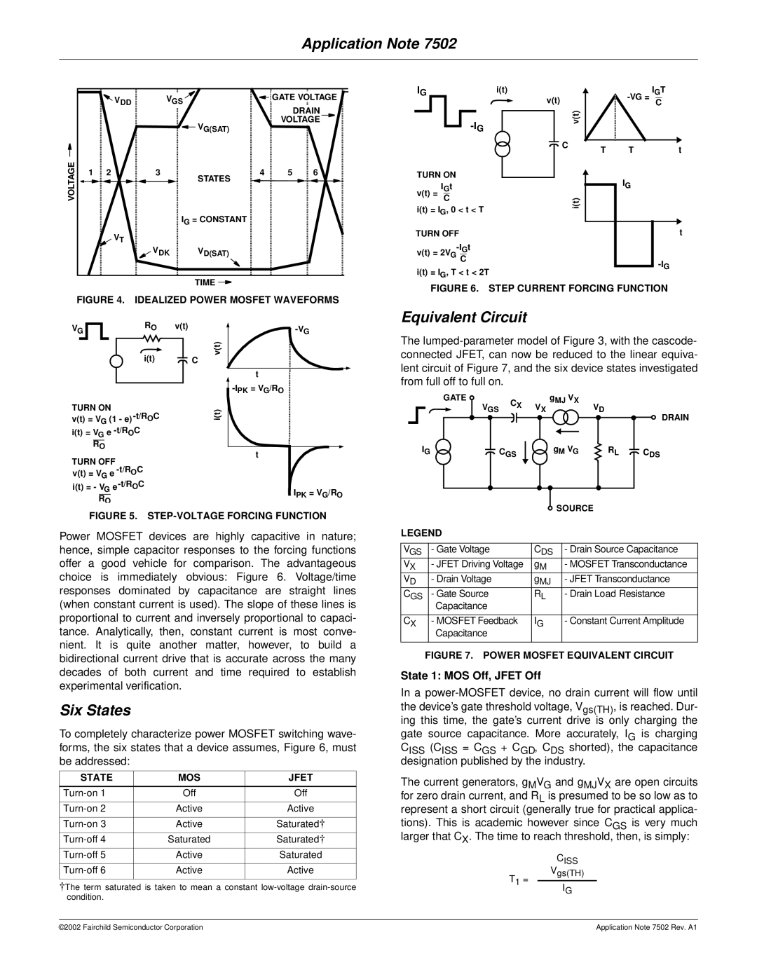
FIGURE 4. IDEALIZED POWER MOSFET WAVEFORMS
FIGURE 6. STEP CURRENT FORCING FUNCTION
V |
|
|
|
| RO | v(t) | |||||
G |
|
|
|
|
|
|
|
|
|
| |
|
|
|
|
|
|
|
|
|
|
|
|
|
|
|
|
|
|
|
|
|
|
|
|
|
|
|
|
|
| i(t) |
|
|
| C | |
|
|
|
|
|
|
|
|
| |||
|
|
|
|
|
|
|
|
|
|
|
|
TURN ON
v(t) = VG (1 - e)
RO
TURN OFF
v(t) = VG e
RO
v(t) |
t |
i(t)
t
IPK = VG/RO
Equivalent Circuit
The
|
|
| GATE |
|
|
|
| CX |
|
| gMJ VX |
|
|
|
|
|
|
|
| ||
|
|
|
| VGS | VX | VD |
|
| DRAIN | ||||||||||||
|
|
|
|
|
|
|
|
|
|
|
|
|
|
|
|
|
|
|
|
| |
|
|
|
|
|
|
|
|
|
|
|
|
|
|
|
|
|
|
|
|
|
|
| IG |
|
|
|
|
| CGS |
|
| gM VG |
|
|
| RL |
|
| CDS | ||||
|
|
|
|
|
|
|
|
|
|
|
|
| |||||||||
|
|
|
|
|
|
|
|
|
|
|
|
| |||||||||
|
|
|
|
|
|
|
|
|
|
|
|
|
|
|
|
|
|
|
|
|
|
|
|
|
|
|
|
|
|
|
|
|
|
|
|
|
|
|
|
|
|
|
|
|
|
|
|
|
|
|
|
|
|
|
| SOURCE |
|
|
| ||||||
|
|
|
|
|
|
|
|
|
|
|
|
|
|
| |||||||
FIGURE 5. STEP-VOLTAGE FORCING FUNCTION
Power MOSFET devices are highly capacitive in nature; hence, simple capacitor responses to the forcing functions offer a good vehicle for comparison. The advantageous choice is immediately obvious: Figure 6. Voltage/time responses dominated by capacitance are straight lines (when constant current is used). The slope of these lines is proportional to current and inversely proportional to capaci- tance. Analytically, then, constant current is most conve- nient. It is quite another matter, however, to build a bidirectional current drive that is accurate across the many decades of both current and time required to establish experimental verification.
Six States
To completely characterize power MOSFET switching wave- forms, the six states that a device assumes, Figure 6, must be addressed:
STATE | MOS | JFET |
|
|
|
Off | Off | |
|
|
|
Active | Active | |
|
|
|
Active | Saturated† | |
|
|
|
Saturated | Saturated† | |
|
|
|
Active | Saturated | |
|
|
|
Active |
| |
|
|
|
†The term saturated is taken to mean a constant
LEGEND |
|
| |
|
|
|
|
VGS | - Gate Voltage | CDS | - Drain Source Capacitance |
VX | - JFET Driving Voltage | gM | - MOSFET Transconductance |
VD | - Drain Voltage | gMJ | - JFET Transconductance |
CGS | - Gate Source | RL | - Drain Load Resistance |
| Capacitance |
|
|
|
|
|
|
CX | - MOSFET Feedback | IG | - Constant Current Amplitude |
| Capacitance |
|
|
|
|
|
|
FIGURE 7. POWER MOSFET EQUIVALENT CIRCUIT
State 1: MOS Off, JFET Off
In a power-MOSFET device, no drain current will flow until
the device’s gate threshold voltage, Vgs(TH), is reached. Dur- ing this time, the gate’s current drive is only charging the
gate source capacitance. More accurately, IG is charging
CISS (CISS = CGS + CGD, CDS shorted), the capacitance designation published by the industry.
The current generators, gMVG and gMJVX are open circuits for zero drain current, and RL is presumed to be so low as to represent a short circuit (generally true for practical applica- tions). This is academic however since CGS is very much larger that CX. The time to reach threshold, then, is simply:
CISS
Vgs(TH)
T1 =
IG
©2002 Fairchild Semiconductor Corporation | Application Note 7502 Rev. A1 |