MB39A104
■PIN DESCRIPTION
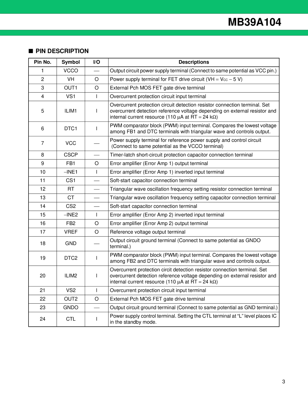
Pin No. | Symbol | I/O | Descriptions | |
|
|
|
| |
1 | VCCO | | Output circuit power supply terminal (Connect to same potential as VCC pin.) | |
|
|
|
| |
2 | VH | O | Power supply terminal for FET drive circuit (VH = VCC − 5 V) | |
|
|
|
| |
3 | OUT1 | O | External Pch MOS FET gate drive terminal | |
|
|
|
| |
4 | VS1 | I | Overcurrent protection circuit input terminal | |
|
|
|
| |
|
|
| Overcurrent protection circuit detection resistor connection terminal. Set | |
5 | ILIM1 | I | overcurrent detection reference voltage depending on external resistor and | |
|
|
| internal current resource (110 ∝A at RT = 24 kΩ) | |
|
|
|
| |
6 | DTC1 | I | PWM comparator block (PWM) input terminal. Compares the lowest voltage | |
among FB1 and DTC terminals with triangular wave and controls output. | ||||
|
|
| ||
|
|
|
| |
7 | VCC | | Power supply terminal for reference power supply and control circuit | |
(Connect to same potential as the VCCO terminal) | ||||
|
|
| ||
|
|
|
| |
8 | CSCP | | ||
|
|
|
| |
9 | FB1 | O | Error amplifier (Error Amp 1) output terminal | |
|
|
|
| |
10 | −INE1 | I | Error amplifier (Error Amp 1) inverted input terminal | |
|
|
|
| |
11 | CS1 | | ||
|
|
|
| |
12 | RT | | Triangular wave oscillation frequency setting resistor connection terminal | |
|
|
|
| |
13 | CT | | Triangular wave oscillation frequency setting capacitor connection terminal | |
|
|
|
| |
14 | CS2 | | ||
|
|
|
| |
15 | −INE2 | I | Error amplifier (Error Amp 2) inverted input terminal | |
|
|
|
| |
16 | FB2 | O | Error amplifier (Error Amp 2) output terminal | |
|
|
|
| |
17 | VREF | O | Reference voltage output terminal | |
|
|
|
| |
18 | GND | | Output circuit ground terminal (Connect to same potential as GNDO | |
terminal.) | ||||
|
|
| ||
|
|
|
| |
19 | DTC2 | I | PWM comparator block (PWM) input terminal. Compares the lowest voltage | |
among FB2 and DTC terminals with triangular wave and controls output. | ||||
|
|
| ||
|
|
|
| |
|
|
| Overcurrent protection circit detection resistor connection terminal. Set | |
20 | ILIM2 | I | overcurrent detection reference voltage depending on external resistor and | |
|
|
| internal current resource (110 ∝A at RT = 24 kΩ) | |
|
|
|
| |
21 | VS2 | I | Overcurrent protection circuit input terminal | |
|
|
|
| |
22 | OUT2 | O | External Pch MOS FET gate drive terminal | |
|
|
|
| |
23 | GNDO | | Output circuit ground terminal (Connect to same potential as GND terminal.) | |
|
|
|
| |
24 | CTL | I | Power supply control terminal. Setting the CTL terminal at “L” level places IC | |
in the standby mode. | ||||
|
|
| ||
|
|
|
|
3