CIRCUIT DESCRIPTION
The
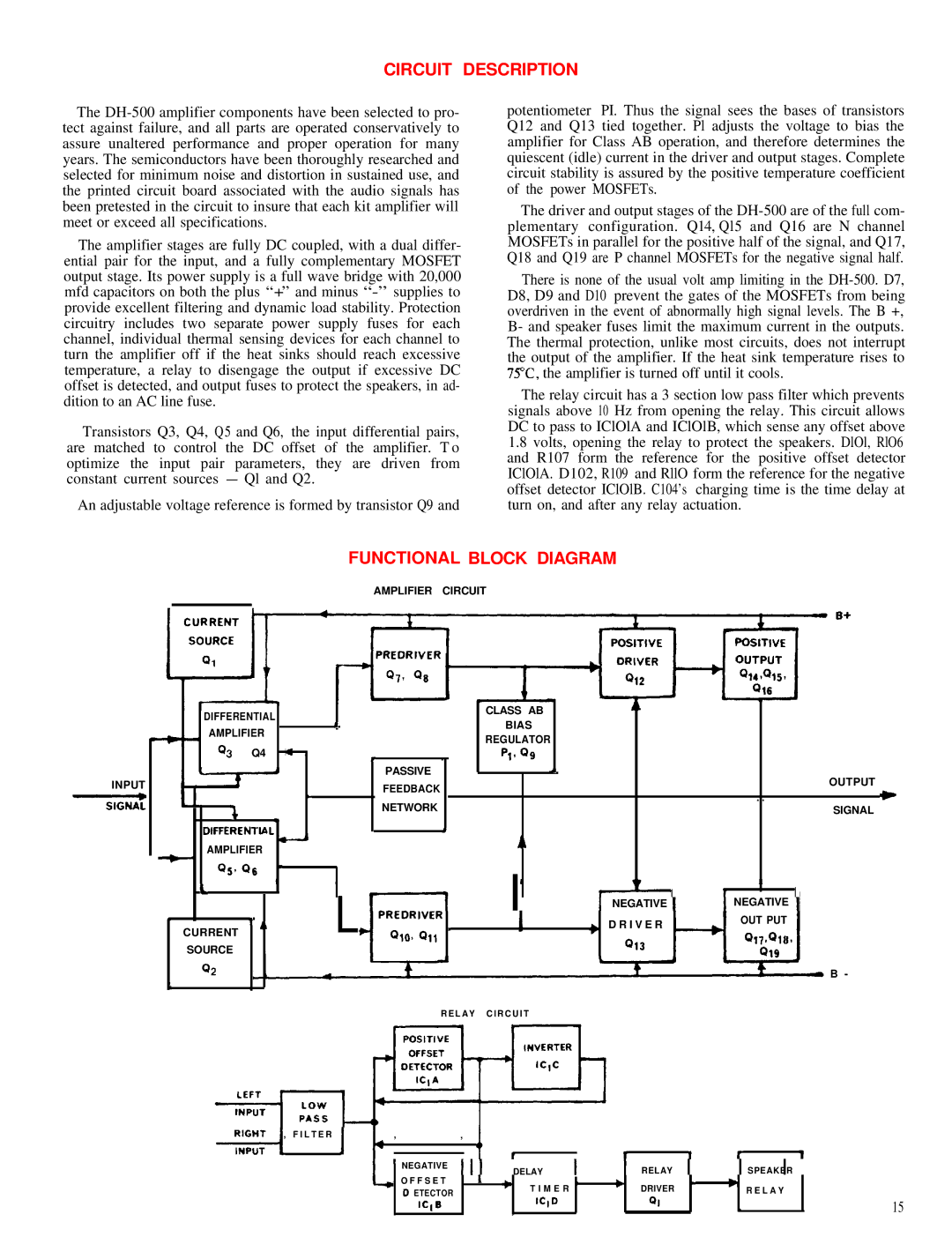
The amplifier stages are fully DC coupled, with a dual differ- ential pair for the input, and a fully complementary MOSFET output stage. Its power supply is a full wave bridge with 20,000 mfd capacitors on both the plus “+” and minus
Transistors Q3, Q4, Q5 and Q6, the input differential pairs, are matched to control the DC offset of the amplifier. T o optimize the input pair parameters, they are driven from constant current sources - Ql and Q2.
An adjustable voltage reference is formed by transistor Q9 and
potentiometer PI. Thus the signal sees the bases of transistors Q12 and Q13 tied together. Pl adjusts the voltage to bias the amplifier for Class AB operation, and therefore determines the quiescent (idle) current in the driver and output stages. Complete circuit stability is assured by the positive temperature coefficient of the power MOSFETs.
The driver and output stages of the
There is none of the usual volt amp limiting in the
The relay circuit has a 3 section low pass filter which prevents signals above 10 Hz from opening the relay. This circuit allows DC to pass to IClOlA and IClOlB, which sense any offset above
1.8volts, opening the relay to protect the speakers. DlOl, RlO6 and R107 form the reference for the positive offset detector IClOlA. D102, R109 and RllO form the reference for the negative offset detector IClOlB. C104’s charging time is the time delay at turn on, and after any relay actuation.
INPUT
FUNCTIONAL BLOCK DIAGRAM
|
|
|
|
|
|
|
|
|
|
|
|
|
| AMPLIFIER | CIRCUIT |
|
|
|
|
|
|
|
|
| |||||
|
|
|
|
|
|
|
|
|
|
|
|
|
|
| rmunlvtn |
|
|
|
|
|
|
|
|
|
|
|
|
|
|
|
|
|
|
|
|
|
|
|
|
|
|
|
|
|
|
|
|
|
|
|
|
|
|
|
|
|
|
| |
|
|
|
|
|
|
|
|
|
|
|
|
|
|
|
|
|
|
|
|
|
|
|
|
|
|
|
| ||
|
|
|
|
|
|
|
|
|
|
|
|
|
|
|
|
|
|
|
|
|
|
|
|
|
|
|
|
|
|
|
|
|
|
|
|
|
|
|
|
|
|
|
|
|
|
|
|
|
|
|
|
|
|
|
|
|
|
|
|
|
|
|
| DIFFERENTIAL |
|
| 0 |
|
|
|
|
| CLASS AB |
|
|
|
|
|
|
|
|
|
|
| |||||
|
|
|
|
|
|
|
|
|
|
|
|
|
|
|
|
|
|
|
|
|
| ||||||||
|
|
|
|
|
|
|
|
|
|
|
|
|
|
|
|
|
|
|
|
|
| ||||||||
|
|
|
|
|
|
|
|
|
|
| BIAS |
|
|
|
|
|
|
|
|
|
|
| |||||||
|
|
|
| AMPLIFIER |
|
|
|
|
|
|
|
|
|
|
|
|
|
|
|
|
|
|
| ||||||
|
|
|
|
|
|
|
|
|
|
|
|
| REGULATOR |
|
|
|
|
|
|
|
|
|
|
| |||||
|
|
|
| 93 |
| Q4 |
| = • |
|
|
|
|
|
|
|
|
|
|
|
|
|
|
|
|
|
| |||
|
|
|
|
|
|
|
|
| r |
| . |
| Pig Q9 |
|
|
|
|
|
|
|
|
|
|
| |||||
|
|
|
|
|
|
|
|
|
|
|
|
|
|
| PASSIVE |
|
| 4 |
|
|
|
|
|
|
|
| OUTPUT | ||
|
|
|
|
|
|
|
|
|
|
|
|
|
|
|
|
|
|
|
|
|
|
|
|
| |||||
|
|
|
|
|
|
|
|
|
|
| c |
|
|
| FEEDBACK |
|
|
|
|
|
|
|
|
|
|
|
| ||
|
|
|
|
|
|
|
|
|
|
|
|
|
|
|
|
|
|
|
|
|
| . | . |
| a | ||||
|
|
|
|
|
|
|
|
|
|
|
|
|
| NETWORK |
|
|
|
|
|
|
|
|
| ||||||
|
|
|
|
|
|
|
|
|
|
|
|
|
|
|
|
|
|
|
|
|
|
| |||||||
|
|
|
|
|
|
|
|
|
|
|
|
|
|
|
|
|
|
|
|
|
|
|
|
|
|
| SIGNAL | ||
|
|
|
| I |
|
|
| I |
|
|
|
|
| 4 |
|
|
|
|
|
|
|
|
|
| |||||
|
|
|
|
|
|
|
|
|
|
|
|
|
|
|
|
|
|
|
|
|
|
|
|
|
| ||||
|
|
|
| DIFFERENTlAL |
|
|
|
|
|
|
|
| ih |
|
|
|
|
|
|
|
|
| |||||||
|
|
|
|
|
|
|
|
|
|
|
|
|
|
|
|
|
|
|
|
| |||||||||
|
|
|
|
|
|
|
|
|
|
|
|
|
|
|
|
|
|
|
|
|
| ||||||||
|
|
|
| AMPLIFIER |
|
|
|
|
|
|
|
|
|
|
|
|
|
|
|
|
|
| |||||||
|
|
|
|
|
|
|
|
|
|
|
|
|
|
|
|
|
|
|
|
|
|
|
|
| |||||
|
|
|
| Q5vQ6 |
| ’ |
|
| 1 |
| I |
|
| 1 |
| r |
| 1 |
| ||||||||||
|
|
|
|
|
|
|
|
|
|
|
|
| |||||||||||||||||
|
|
|
| L |
|
|
|
|
|
|
|
|
|
|
|
|
| ||||||||||||
? |
|
|
|
|
|
|
|
|
|
|
|
|
|
| PREDRIVER |
|
|
|
|
| NEGATIVE 1 | 1 NEGATIVE | 1 |
| |||||
|
|
|
|
|
|
|
|
|
|
|
|
|
|
|
|
|
|
|
|
|
|
|
|
|
|
| |||
|
| CURRENT | t | ,, |
|
|
| L QlO* Qll |
| L | ! |
|
| + | D R I V E R |
| OUT PUT |
|
|
| |||||||||
|
|
|
|
|
|
|
|
|
|
|
|
|
| 913 |
| Q171Q11 |
|
|
| ||||||||||
|
| SOURCE |
|
|
|
|
|
|
|
|
|
|
|
|
|
|
|
|
|
| Qlq |
|
|
| |||||
42 |
|
|
|
|
|
|
|
|
|
|
|
|
|
|
|
|
|
|
|
|
|
|
| B - | |||||
&.
R E L A Y C I R C U I T
a, F I L T E R ] k ,, + ~
|
|
|
|
|
|
|
|
|
|
|
|
|
| t |
| I |
| r |
| 1 | ||
|
|
|
|
|
|
|
|
|
|
|
|
|
|
|
| |||||||
I I | NEGATIVE | 1 1 1 |
| DELAY | f | I | RELAY | I | I | SPEAKER |
| |||||||||||
|
|
| ||||||||||||||||||||
|
|
| I |
| ||||||||||||||||||
I | O F F S E T |
| 1 | + |
| T I M E R |
|
|
|
| DRIVER |
|
|
|
| R E L A Y |
| |||||
|
|
| 0 ETECTOR |
|
|
|
|
|
|
|
| ’ | + | r | D |
|
|
| ||||
|
|
| lC[B |
|
|
|
|
| , | ICl D | . |
|
| Ql |
|
|
| • |
|
| ||
15