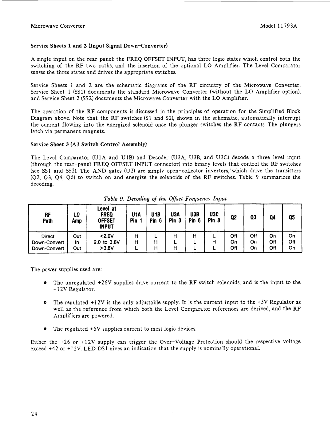
11793A specifications
The HP 11793A is a precision electronic component designed for high-frequency signal processing and transmission, primarily used in laboratory and industrial applications. This device exemplifies HP's longstanding commitment to quality and innovation in the world of electronic instrumentation.One of the notable features of the HP 11793A is its ability to handle a wide frequency range, making it suitable for a variety of tasks, including signal analysis, modulation, and demodulation. This versatility is complemented by its excellent linearity and low distortion, which are critical factors for applications that require high accuracy and reliability in signal representation.
The HP 11793A employs advanced technologies that enhance its performance and usability. One of the key technologies is its robust signal conditioning capabilities, which allow it to filter and amplify signals effectively. This ensures that even weak signals can be accurately processed, significantly improving measurement reliability. Furthermore, the device uses cutting-edge materials and manufacturing processes to minimize noise and interference, paving the way for clearer and more precise signal outputs.
Another significant aspect of the HP 11793A is its user-friendly interface. Designed with the operator in mind, the device features intuitive controls and a well-organized display, enabling quick adjustments and easy monitoring of parameters. This ergonomic design is particularly beneficial in high-pressure environments where time is crucial, allowing technicians and engineers to focus on their tasks without being bogged down by complicated procedures.
Reliability is paramount in any electronic component, and the HP 11793A does not disappoint. Built to withstand rigorous testing and prolonged usage, it boasts a durable construction that ensures longevity. The device also adheres to strict safety and performance standards, providing users with peace of mind.
In conclusion, the HP 11793A combines high-frequency signal processing capabilities, advanced signal conditioning technologies, user-friendly design, and robust reliability. These features make it an essential tool for professionals in the fields of electronics, telecommunications, and research laboratories, contributing to a more efficient and effective workflow in high-precision tasks. Whether for development, testing, or analysis, the HP 11793A stands out as a notable choice in the realm of electronic instrumentation.

