2
Chapter 2. Architecture and technical overview
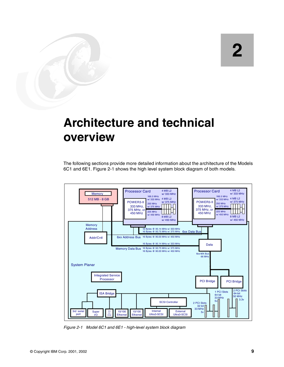
The following sections provide more detailed information about the architecture of the Models 6C1 and 6E1. Figure
|
|
|
|
|
|
| Processor Card | 4 MB L2 |
|
| Processor Card | 4 MB L2 |
| |||||||||||||||||||||||
|
| Memory |
|
|
|
|
|
|
| 166.5 MHz | w/ 333 MHz |
|
|
|
|
|
|
| 166.5 MHz | w/ 333 MHz |
| |||||||||||||||
|
| 512 MB - 8 GB |
|
|
|
|
|
|
| 4 MB L2 |
|
|
|
|
|
|
| 4 MB L2 |
| |||||||||||||||||
|
|
|
|
|
|
|
|
| w/ 333 MHz |
|
|
|
|
|
|
| w/ 333 MHz |
| ||||||||||||||||||
|
|
|
|
|
|
|
| 250 MHz | w/ 375 MHz |
|
| POW | 250 MHz | w/ 375 MHz |
| |||||||||||||||||||||
|
|
|
|
|
|
| 333 MHz, | w/ 375 MHz |
|
|
|
|
|
|
|
|
|
| 333 MHz, | w/ 375 MHz |
|
|
|
|
|
|
|
| ||||||||
|
|
|
|
|
|
| 375 MHz, or |
|
|
|
|
|
|
|
|
|
| 375 MHz, or |
|
|
|
|
|
|
|
|
|
| ||||||||
|
|
|
|
|
|
| 225 MHz |
|
|
|
|
|
|
|
|
| 225 MHz |
|
|
|
|
|
|
|
| |||||||||||
|
|
|
|
|
|
| 450 MHz |
|
|
|
|
|
|
|
|
|
| 450 MHz |
|
|
|
|
|
|
|
| ||||||||||
|
|
|
|
|
|
|
|
|
|
|
| w/ 450 MHz |
|
|
|
|
|
|
|
|
|
|
|
|
|
| w/ 450 MHz |
|
|
|
|
|
|
|
| |
|
|
|
|
|
|
|
|
|
|
|
| 8 MB L2 |
|
|
|
|
|
|
| 8 MB L2 |
| |||||||||||||||
|
|
|
|
|
|
|
|
|
|
|
|
|
|
|
|
|
|
|
|
|
|
| ||||||||||||||
|
|
|
|
|
|
|
|
|
|
|
|
| w/ 450 MHz |
|
|
|
|
|
|
|
|
| w/ 450 MHz |
| ||||||||||||
|
| Memory |
|
|
|
|
|
|
|
|
|
|
|
|
|
|
|
|
|
|
|
|
|
|
|
|
|
|
|
|
|
|
|
|
|
|
|
| Address |
|
|
|
|
|
|
|
|
|
|
|
|
|
|
|
|
|
|
|
|
|
|
|
|
|
|
|
|
|
|
|
|
|
|
|
|
|
|
|
|
|
|
| 16 Bytes @ 95.14 MHz w/ 333 MHz | 6xx Data Bus |
|
|
|
|
|
|
|
|
|
|
|
|
| |||||||||||||
|
|
|
|
|
|
|
|
|
| 16 Bytes @ 93.75 MHz w/ 375 MHz |
|
|
|
|
|
|
|
|
|
|
|
|
| |||||||||||||
|
| Addr/Cntl |
| 6xx Address Bus 16 Bytes @ 90.00 MHz w/ 450 MHz |
|
|
|
|
|
|
|
|
|
|
|
|
|
|
|
| ||||||||||||||||
|
|
|
|
|
|
|
|
|
| 16 Bytes @ 95.14 MHz w/ 333 MHz |
|
|
| Data |
|
|
|
|
|
|
|
|
|
| ||||||||||||
|
|
|
|
|
|
|
|
|
|
|
|
|
|
|
|
|
|
|
| |||||||||||||||||
|
|
|
|
| Memory Data Bus 16 Bytes @ 93.75 MHz w/ 375 MHz |
|
|
|
|
|
|
|
|
|
|
|
|
|
|
|
| |||||||||||||||
|
|
|
|
|
|
|
|
|
| 16 Bytes @ 90.00 MHz w/ 450 MHz |
|
|
|
|
|
|
|
|
|
|
|
|
|
|
|
| ||||||||||
|
|
|
|
|
|
|
|
|
|
|
|
|
|
|
|
|
| |||||||||||||||||||
|
|
|
|
|
|
|
|
|
|
|
|
|
|
|
|
|
|
|
|
|
|
|
|
|
|
|
|
|
|
|
| |||||
|
|
|
|
|
|
|
|
|
|
|
|
|
|
|
|
|
|
|
|
|
|
| 66 MHz |
|
|
|
|
|
|
|
|
|
| |||
System Planar |
|
|
|
|
|
|
|
|
|
|
|
|
|
|
|
|
|
|
|
|
|
|
|
|
|
|
|
|
|
|
|
| ||||
Integrated Service
Processor
PCI Bridge
PCI Bridge
ISA Bridge |
3rd serial | Super | IDE | 10/100 | 10/100 |
port | I/O | CD- | Ethernet | Ethernet |
ROM |
SCSI Controller
Internal |
| External |
| ||
|
|
|
2 PCI Slots
32bit 33 MHz 5v
1 PCI Slots
64bit
33MHz
5v
2 PCI Slots
50MHz 3.3v
Figure 2-1 Model 6C1 and 6E1 - high-level system block diagram
© Copyright IBM Corp. 2001, 2002 | 9 |