SECTION 4 CIRCUIT DESCRIPTION
4-1 RECEIVER CIRCUITS
4-1-1 ANTENNA SWITCHING CIRCUIT
Received signals are passed through the
The antenna switching circuit functions as a
4-1-2 RF CIRCUIT
The RF circuit amplifies signals within the range of frequen- cy coverage and filters
The signals from the antenna switching circuit are amplified at the RF amplifier (Q12) after passing through the tunable bandpass filter (D9, D10, L16, L17,
Varactor diodes are employed at the bandpass filters that track the filters and are controlled by the CPU (IC8) via the expander IC (IC10) using
The signals from the RF circuit are mixed at the 1st mixer (Q13) with a 1st LO signal coming from the VCO circuit to produce a 31.05 MHz 1st IF signal.
The 1st IF signal is applied to two crystal filters (FI1) to sup- press
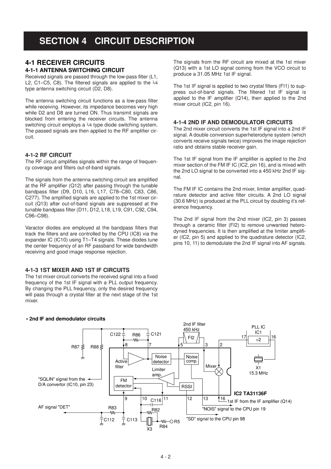
4-1-4 2ND IF AND DEMODULATOR CIRCUITS
The 2nd mixer circuit converts the 1st IF signal into a 2nd IF signal. A double conversion superheterodyne system (which converts receive signals twice) improves the image rejection ratio and obtains stable receiver gain.
The 1st IF signal from the IF amplifier is applied to the 2nd mixer section of the FM IF IC (IC2, pin 16), and is mixed with the 2nd LO signal to be converted into a 450 kHz 2nd IF sig- nal.
The FM IF IC contains the 2nd mixer, limiter amplifier, quad- rature detector and active filter circuits. A 2nd LO signal (30.6 MHz) is produced at the PLL circuit by doubling it’s ref- erence frequency.
The 2nd IF signal from the 2nd mixer (IC2, pin 3) passes through a ceramic filter (FI2) to remove unwanted hetero- dyned frequencies. It is then amplified at the limiter amplifi- er (IC2, pin 5) and applied to the quadrature detector (IC2, pins 10, 11) to demodulate the 2nd IF signal into AF signals.
4-1-3 1ST MIXER AND 1ST IF CIRCUITS
The 1st mixer circuit converts the received signal into a fixed frequency of the 1st IF signal with a PLL output frequency. By changing the PLL frequency, only the desired frequency will pass through a crystal filter at the next stage of the 1st mixer.
• 2nd IF and demodulator circuits
|
|
|
|
|
| 2nd IF filter |
| PLL IC |
|
|
|
|
|
|
| 450 kHz |
|
| |
|
| C122 |
| C121 |
|
| IC1 |
| |
|
| R86 |
|
| 17 | 16 | |||
|
|
| FI2 | ⋅2 | |||||
|
|
|
|
|
| ||||
|
| 8 |
| 7 | 5 | 3 | 2 |
| |
R87 | R88 |
|
|
| |||||
|
|
|
|
|
|
|
| ||
|
|
|
| Noise |
| Noise |
|
|
|
|
| Active |
| detector |
| comp. |
|
|
|
|
| filter |
| Limiter |
| Mixer |
| X1 |
|
|
|
|
|
|
|
| 15.3 MHz |
| |
|
|
|
| amp. |
|
|
|
| |
|
|
|
|
|
|
|
|
|
"SQLIN" signal from the |
| FM |
|
|
|
|
|
|
|
D/A convertor (IC10, pin 23) |
|
|
|
|
|
|
|
| |
| detector |
|
|
|
| RSSI |
|
| |
|
|
|
|
|
|
|
| ||
|
|
|
|
|
|
|
|
| IC2 TA31136F |
|
| 9 | 10 | C116 11 |
| 12 | 13 | 16 1st IF from the IF amplifier (Q14) | |
AF signal "DET" | R83 |
| R82 |
|
| "NOIS" signal to the CPU pin 19 | |||
|
|
|
| ||||||
| C112 | C113 |
|
|
| R5 | "SD" signal to the CPU pin 98 | ||
|
|
|
|
| R84 |
|
|
| |
|
|
| X3 |
|
|
|
| ||
|
|
|
|
|
|
|
| ||
4 - 2