The signal output from the power detector circuit (D32, D33) is applied to the differential amplifier (IC3a, pin 2), and the “T4” signal from the expander (IC10, pin 11), controlled by the CPU (IC8), is applied to the other input for reference.
When the driving current is increased, input voltage of the differential amplifier (pin 2) will be increased. In such cases, the differential amplifier output voltage (pin 1) is decreased to reduce the driving current.
4-3 PLL CIRCUIT
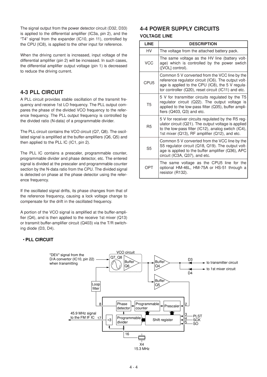
A PLL circuit provides stable oscillation of the transmit fre- quency and receive 1st LO frequency. The PLL output com- pares the phase of the divided VCO frequency to the refer- ence frequency. The PLL output frequency is controlled by the divided ratio
The PLL circuit contains the VCO circuit (Q7, Q8). The oscil- lated signal is amplified at the
The PLL IC contains a prescaler, programmable counter, programmable divider and phase detector, etc. The entered signal is divided at the prescaler and programmable counter section by the
If the oscillated signal drifts, its phase changes from that of the reference frequency, causing a lock voltage change to compensate for the drift in the oscillated frequency.
A portion of the VCO signal is amplified at the
 PLL CIRCUIT
4-4 POWER SUPPLY CIRCUITS VOLTAGE LINE
LINE | DESCRIPTION | |
|
| |
HV | The voltage from the attached battery pack. | |
|
| |
| The same voltage as the HV line (battery volt- | |
VCC | age) which is controlled by the power swtich | |
| ([VOL] control). | |
|
| |
| Common 5 V converted from the VCC line by the | |
CPU5 | reference regulator circuit (IC6). The output volt- | |
age is applied to the CPU (IC8), the 5 V regula- | ||
| ||
| tor controller (Q20), reset circuit (IC11) and etc. | |
|
| |
| 5 V for transmitter circuits regulated by the T5 | |
T5 | regulator circuit (Q22). The output voltage is | |
applied to the | ||
| ||
| fiers (Q403, Q3) and etc. | |
|
| |
| 5 V for receiver circuits regulated by the R5 reg- | |
R5 | ulator circuit (Q21). The output voltage is applied | |
to the | ||
| ||
| 1st mixer (Q13), RF amplifier (Q12), and etc. | |
|
| |
| Common 5 V converted from the VCC line by the | |
S5 | S5 regulator circuit (Q18, Q19). The output volt- | |
age is applied to the buffer amplifier (Q36), APC | ||
| ||
| circuit (IC3A, Q37), and etc. | |
|
| |
| The same voltage as the CPU5 line for the | |
OPT | optional | |
| resistor (R132). | |
|
|
"DEV" signal from the
D/A convertor (IC10, pin 22) when transmitting
Loop
filter
VCO circuit
Q7, Q8
Buffer Q6
![]() Buffer
Buffer
Q4
Buffer
Q5
D3
![]() to transmitter circuit
to transmitter circuit
![]() to 1st mixer circuit D4
to 1st mixer circuit D4
45.9MHz signal to the FM IF IC
8 |
| Phase | Programmable | Prescaler | 2 |
| ||
|
| detector | counter |
|
|
| ||
|
|
|
|
|
| |||
17 |
| Programmable |
|
| 3 | PLST | ||
3 | Shift register | 4 | ||||||
SCK | ||||||||
| divider |
| 5 | |||||
|
|
|
|
| SO | |||
|
|
|
|
|
|
| ||
|
| 16 |
|
|
|
|
| |
X4
15.3 MHz
4 - 4
