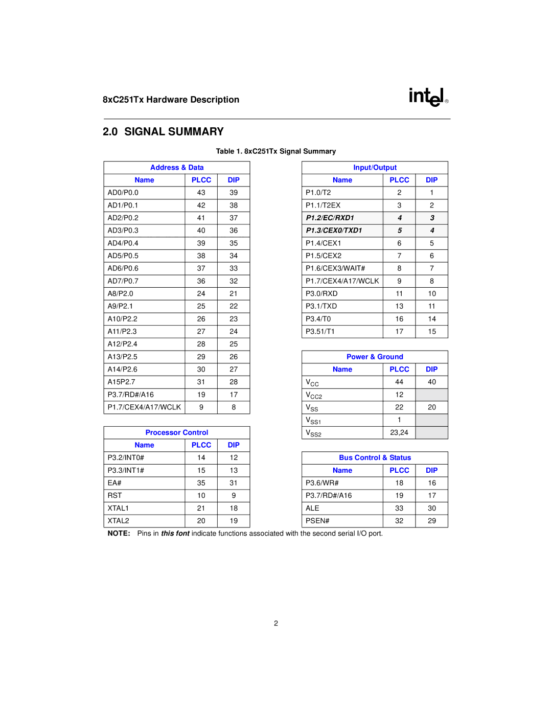
8XC251SP, 8XC251SA, 8XC251SQ, 8xC251TB, 8xC251TQ specifications
The Intel 8XC251 series of embedded microcontrollers is a family of versatile and powerful devices, designed to meet the demands of a wide range of applications. With models such as the 8XC251SB, 8XC251SQ, 8XC251SA, and 8XC251SP, this series offers unique features while maintaining a high level of performance and reliability.At the heart of the 8XC251 microcontrollers is the 8051 architecture, which provides a 16-bit processor capable of executing complex instructions efficiently. This architecture not only allows for a rich instruction set but also facilitates programming in assembly language and higher-level languages like C, which are essential for developing sophisticated embedded systems.
One of the significant features of the 8XC251 family is its integrated peripherals, including timer/counters, serial communication interfaces, and interrupt systems. These peripherals enable developers to implement timing functions, data communication, and real-time processing, all of which are crucial in modern embedded applications. The 8XC251SB and 8XC251SQ models, for instance, come equipped with multiple I/O ports that allow for interfacing with other devices and systems, enhancing their functionality in various environments.
The memory architecture of the 8XC251 devices is noteworthy, featuring on-chip ROM, RAM, and EEPROM. The on-chip memory allows for fast access times, which is essential for executing programs efficiently. Moreover, the EEPROM serves as non-volatile memory, enabling the storage of configuration settings and important data that must be retained even when power is lost.
In terms of operating voltage, the 8XC251 devices are designed to operate in a wide range, typically between 4.0V and 6.0V. This flexibility makes them suitable for battery-powered applications, where energy efficiency is critical. The power management features, including reduced power modes, further enhance their suitability for portable devices.
Lastly, the 8XC251 series is supported by a wide range of development tools and resources, allowing engineers and developers to streamline the development process. This support, combined with the microcontrollers' robust features, makes the Intel 8XC251 family a reliable choice for various embedded applications, such as industrial automation, automotive systems, and consumer electronics.
Overall, the Intel 8XC251SB, 8XC251SQ, 8XC251SA, and 8XC251SP deliver high performance, versatility, and ease of use, making them a preferred choice for embedded system designers looking to develop efficient and effective solutions.

