Mobile Intel® 915GME Express Chipset
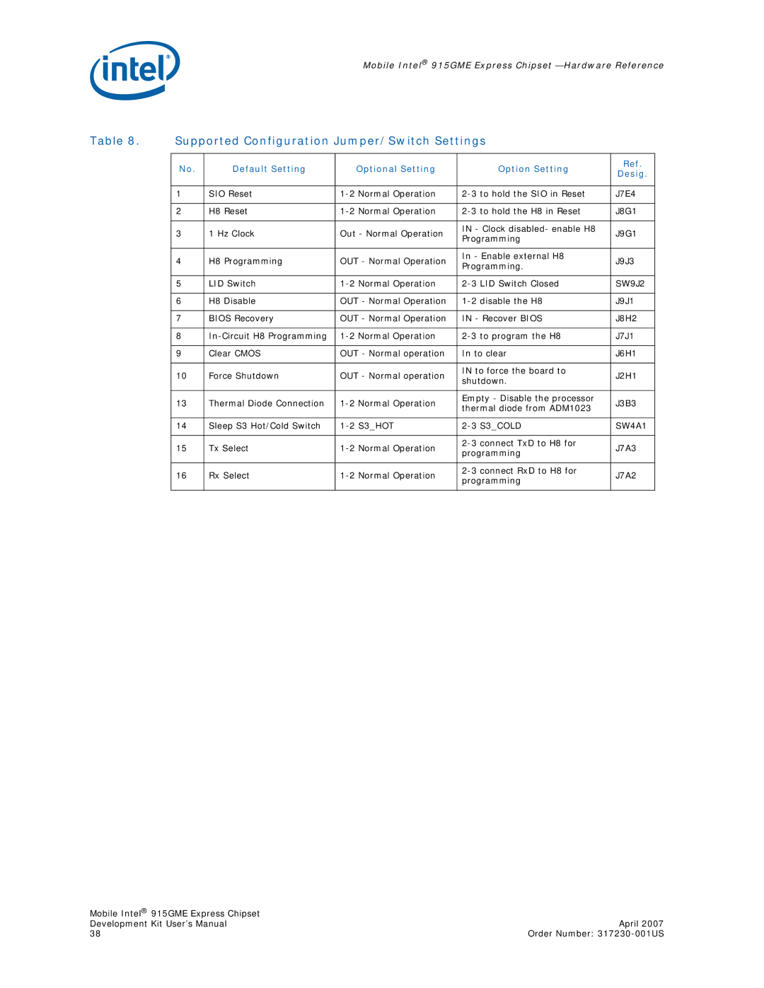
Table 8. | Supported Configuration Jumper/Switch Settings |
| |||
|
|
|
|
|
|
| No. | Default Setting | Optional Setting | Option Setting | Ref. |
| Desig. | ||||
|
|
|
|
| |
|
|
|
|
|
|
| 1 | SIO Reset | J7E4 | ||
|
|
|
|
|
|
| 2 | H8 Reset | J8G1 | ||
|
|
|
|
|
|
| 3 | 1 Hz Clock | Out - Normal Operation | IN - Clock disabled- enable H8 | J9G1 |
| Programming | ||||
|
|
|
|
| |
|
|
|
|
|
|
| 4 | H8 Programming | OUT - Normal Operation | In - Enable external H8 | J9J3 |
| Programming. | ||||
|
|
|
|
| |
|
|
|
|
|
|
| 5 | LID Switch | SW9J2 | ||
|
|
|
|
|
|
| 6 | H8 Disable | OUT - Normal Operation | J9J1 | |
|
|
|
|
|
|
| 7 | BIOS Recovery | OUT - Normal Operation | IN - Recover BIOS | J8H2 |
|
|
|
|
|
|
| 8 | J7J1 | |||
|
|
|
|
|
|
| 9 | Clear CMOS | OUT - Normal operation | In to clear | J6H1 |
|
|
|
|
|
|
| 10 | Force Shutdown | OUT - Normal operation | IN to force the board to | J2H1 |
| shutdown. | ||||
|
|
|
|
| |
|
|
|
|
|
|
| 13 | Thermal Diode Connection | Empty - Disable the processor | J3B3 | |
| thermal diode from ADM1023 | ||||
|
|
|
|
| |
|
|
|
|
|
|
| 14 | Sleep S3 Hot/Cold Switch | SW4A1 | ||
|
|
|
|
|
|
| 15 | Tx Select | J7A3 | ||
| programming | ||||
|
|
|
|
| |
|
|
|
|
|
|
| 16 | Rx Select | J7A2 | ||
| programming | ||||
|
|
|
|
| |
|
|
|
|
|
|
Mobile Intel® 915GME Express Chipset |
|
Development Kit User’s Manual | April 2007 |
38 | Order Number: |