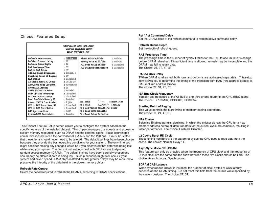
Chipset Features Setup
ROM PCI/ISA BIOS (2A5IMTPD)
CHIPSET FEATURES SETUP
AWARD SOFTWARE, INC.
|
|
|
|
|
|
|
Refresh Rate Control | : | 15.6us |
| Video BIOS Cachable | : Enabled | |
Ref/Act Command delay | : | 6T |
| Memory Hole at 15/16M | : Enabled | |
Refresh Queue Depth | : 12 |
| PCI Post Write Buffer | : Disabled | ||
RAS Precharge Time | : 3T |
| PCI Delayed Transaction | : Disabled | ||
RAS to CAS Delay | : 3T |
|
|
|
| |
ISA Bus Clock Frequency | : PCICLK/4 |
|
|
|
| |
Starting Point of Paging | : 1T |
|
|
|
| |
NA# Enable | : Disabled |
|
|
|
| |
L2 Cache Burst RD Cycle | : Delay 1T |
|
|
|
| |
Asyn/Sync Mode CPU DRAM | : Asynchron |
|
|
|
| |
SDRAM CAS Latency | : 3T |
|
|
|
| |
SDRAM WR Retite Rate | : |
|
|
|
| |
DRAM Opt RAS Precharge | : Disabled |
|
|
|
| |
PCI Peer Concurrency | : Disabled |
|
|
|
| |
Read Prefetch Memory RD | : Enabled |
|
|
|
| |
| Esc: Quit |
| : Select Item | |||
Assert TRDY After Prefet | : 2 QWs |
| − ↓ → ← | |||
CPU to PCI Burst Mem. WR | : Disabled |
| F1 : Help | |||
CPU to PCI Post Write | : Disabled |
| F5 : Old Values (Shift)F2: Color | |||
AGP Aperture Size | : 64MB |
| F6 : Load BIOS Defaults |
| ||
System BIOS Cacheable | : Enabled |
| F7 : Load Setup Defaults |
| ||
This Chipset Feature Setup screen allows you to configure the system based on the specific features of the installed chipset. This chipset manages bus speeds and access to system memory resources, such as DRAM and the external cache. It also coordinates communications between the conventional ISA bus and the PCI bus. It must be stated that these items should never need to be altered. The default settings have been chosen because they provide the best operating conditions for your system. The only time you might consider making any changes would be if you discovered that data was being lost while using your system. The first chipset settings deal with CPU access to dynamic random access memory (DRAM). The default timings have been carefully chosen and should only be altered if data is being lost. Such a scenario might well occur if your system had mixed speed DRAM chips installed so that greater delays may be required to preserve the integrity of the data held in the slower memory chips.
Refresh Rate Control
Select the period required to refresh the DRAMs, according to DRAM specifications.
Ref / Act Command Delay
Set the DRAM clock of the refresh command to refresh/active command delay.
Refresh Queue Depth
Set the depth of refresh queue.
RAS Precharge Time
The precharge time is the number of cycles it takes for the RAS to accumulate its charge before DRAM refreshes. If insufficient time is allowed, refresh may be incomplete and the DRAM may fail to retain data.
The Choice: 2T, 3T, 4T, 5T.
RAS to CAS Delay
TWhen DRAM is refreshed, both rows and columns are addressed separately. This setup item allows you to determine the timing of the transition from RAS (row address strobe) to CAS (column address strobe).
The choice: 2T, 3T, 4T, 5T.
ISA Bus Clock Frequency
You can set the speed of the AT bus at
Starting Point of Paging
This value controls the start timing of memory paging operations.
The choice: 1T, 2T, 4T, 8T.
NA# Enable
Selecting Enabled permits pipelining, in which the chipset signals the CPU for a new memory address before all data transfers for the current cycle are complete, resulting in faster performance. The choice: Enabled, Disabled.
L2 Cache Burst RD Cycle
These timing numbers are the pattern of cycles the CPU uses to read data from the cache. The choice: Normal, Delay 1T.
Asyn/Sync Mode CPU/DRAM
This feature can only be enabled when the frequency of CPU clock and the frequency of DRAM clock are the same and the skew between these two clocks should be zero. The choice: Asynchronous, Synchronous.
SDRAM CAS Latency
When synchronous DRAM is installed, the number of clock cycles of CAS latency depends on the DRAM timing. Do not reset this field from the default value specified by the system designer. The choice: 2T, 3T.
18 |