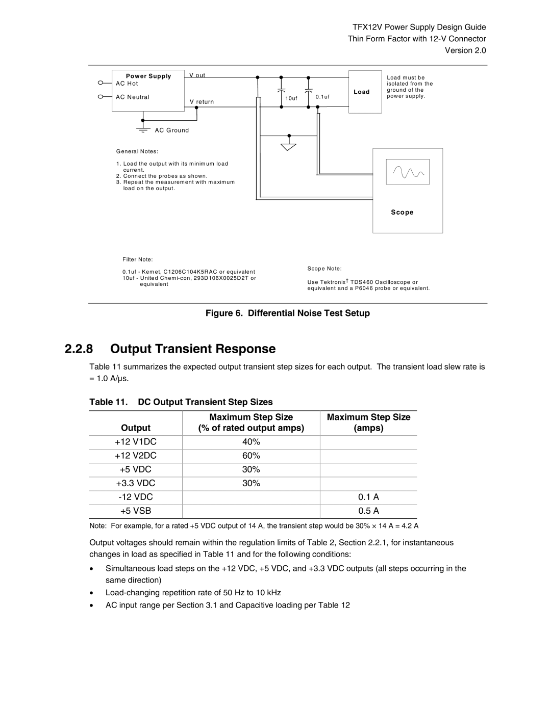
TFX12V specifications
The Intel TFX12V is a power supply unit (PSU) designed specifically for compact desktop systems, catering to the needs of PC builders who prioritize space-efficient components without compromising on performance. Intel's TFX12V specification defines the form factor and power delivery standards, ensuring compatibility across a wide range of motherboards and peripherals.One of the main features of the TFX12V is its slimline design. Measuring 85mm in height, 65mm in width, and 150mm in depth, this PSU fits into smaller case designs, making it ideal for compact desktops or media centers. Despite its small size, the TFX12V delivers robust power, typically ranging from 300W to 400W. This output is sufficient for everyday computing tasks, light gaming, and media consumption, allowing users to create space-saving systems without sacrificing functionality.
The TFX12V power supply adheres to the ATX power supply standard, featuring a 24-pin ATX connector, which ensures broad compatibility with modern motherboards. Additionally, the TFX12V includes connections for other crucial components, such as the 4-pin CPU power connector and multiple SATA and PCIe connectors, enabling the build of systems with modern graphics cards and storage solutions.
The efficiency of the TFX12V is another significant aspect. Many models are designed to meet or exceed the 80 PLUS certification, which indicates at least 80% efficiency at 20%, 50%, and 100% loads. High efficiency not only reduces energy consumption but also minimizes heat generation, leading to quieter operation due to lower fan speeds.
In terms of safety and reliability, TFX12V power supplies come equipped with standard protections against over-voltage, under-voltage, and short-circuits. These safety features safeguard the valuable components of a PC from potential power surges or failures.
Furthermore, the product lifecycle of the Intel TFX12V often ensures access to advanced technologies, including pulsating load regulation and enhanced thermal management technologies. These features contribute to a stable power output and improved performance, even under load.
In summary, the Intel TFX12V power supply unit combines compactness, efficiency, and reliability, making it an attractive choice for users looking to build a small form-factor PC without compromising on essential features or quality. With its robust performance and modern technology, it meets the demands of today's computing needs effectively.

