Lucent Technologies USS-720 Parallel, Port, Bridging USB to, Typical Circuit Showing, the USS

Models: USS-720

1 96
Download 96 pages 16.83 Kb
Page 57
Image 57
5V_pullup

Lucent


TechnologiesInc.


4

3

2

1

6-3

A

Sufficient grounding must be implemented on the board to ensure proper functionality. A 4-layer board design is recommended with two layers for power and ground planes.

CONNECTOR CENT36

J1

19

1

nSTROBE

20

2

Data_0

21

3

Data_1

22

4

Data_2

23

5

Data_3

24

6

Data_4

25

7

Data_5

26

8

Data_6

27

9

Data_7

2810 nACK

2911 BUSY

3012 PError

3113 SELECT

3214 nAUTOFD

3315

3416

3517

3618PLH

nSELECTIN

nFAULT

nINIT

A


B


C


D


VCC_5V


VCC


U?


D1


8

VCC


CS

1


DIODE


U1


7


2


nc


SK


LT1121CST_3.3


5V_pullup


6

nc


DI

3


VCC

3

VOUT

VIN

1


5

GND


DO

4


GND


C11

1


4


R1

R2

R3

R4

R5

R6

R7


+


2


2


93CS56


VCC

C1


C2 +


3.3ufd tant.


.01ufd


3.3ufd tant.


R8


44

43

42

41

40

39

38

37

36

35

34


VCC


C3

C4


.1ufd

.1ufd


D0

nSTROBE HLH PLH

Suspend GND VCC nUSB Reset DIO

CS SK


PLH


R10


1

D1


tst_rst

33


1.5k


2


32


R11


24

Data_0

VDD_5V


D2


reset


1

2


3


31


VDD_5V


test


R13


J2


R12

1

2

24

Data_1


4


30

VCC


Data_2


D3


GND

24

2


VCC_5V

1

3


R14

1

2

24


5

D4


U2

VCC

29

1


RED


R15

1

2

24

Data_3


6


28


DATA-

2


GND


DMNS


WHITE


R17

1

2

24

Data_4


7


27

1


2


DATA+

3


D5


DPLS


GREEN


R18

1

2

24

Data_5


8


26


24


GND

4


VDD_5V


D6


PLL_VSS


R16


BLACK


R19

1

2

24

Data_6


9


25


5


VDD_5V


PLL_VDD


SHIELD


R20

1

2

24

Data_7


10


24

1


D7


SCAN_EN


11


23

C5


CON5


nAUTOFD


SCAN


nACK

VCC


nSELECTIN


.1ufd


BUSY


nINIT nACK BUSY

VCC GND PEerror SELECT nFAULT

LOCLK HICLK

QUAD_44_p

2


PError


SELECT


nFAULT


R21

1

2

24

nSTROBE


12 13

14

15 16

17 18

19

20 21

22


R22

1

2

24

nAUTOFD


R23

1

2

24

nSELECTIN


R24

1

2

24

nINIT


Standard decoupling should be used on the


board. 0.1ufd capacitors between VCC_5V, VCC,


and GND placed as close as possible to the


R33

R32

R31

R30

R29

R28

R27

R26

R25


EEPROM

power pins on the USS-720 is recommended.


2


VCC


VCC


5V_pullup


ASIC BYPASS


CRYSTAL


C13


C12


C8


C9


C10


C6


Y1

C7


.1ufd


.1ufd


.1ufd


.1ufd


.1ufd


15 pf


15 pf


In-System Design, Inc.


1


The schematic provided with the


Boise, Idaho


Evaluation Kit is for reference only.


It’s suitability for use for any


Title


particular purpose is not warrented by


ISD-101

USB to Parallel 1284


Lucent or In-System Design.


Size

Document Number


Rev


B

{Doc}


B


Copywrite 1997, 1998, In-System Design Inc.


Date:

Wednesday, June 24, 1998


Sheet

1


of

1


B


C


D


Figure 1. USS-720 Evaluation Kit Schematic

Application Note February 1999

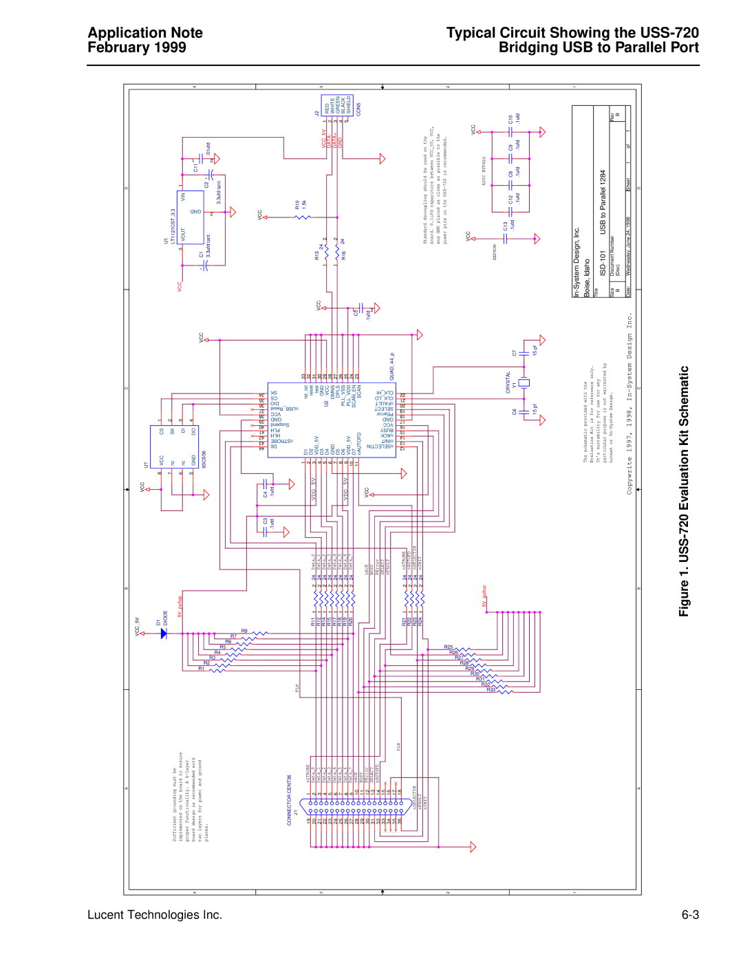
Bridging USB to

Typical Circuit Showing

Parallel

the USS

-720 Port

Page 57
Image 57
Lucent Technologies USS-720 Parallel, Port, Bridging USB to, Typical Circuit Showing, the USS, Application Note February