Page
USB-1616HS-2
Management committed to your satisfaction
Trademark and Copyright Information
Table of Contents
USB-1616HS-2 Users Guide
What you will learn from this users guide
Where to find more information
About this Users Guide
Conventions used in this users guide
Introducing the USB-1616HS-2
Overview USB-1616HS-2 features
Software features
Chapter
What comes with your USB-1616HS-2 shipment?
Installing the USB-1616HS-2
TR-2U power supply and CA-1* line cord
Hardware
Additional documentation
Installing the software
Unpacking the USB-1616HS-2
CA-96A expansion cable
Installing the hardware
Connectors, cables main I/O connector
Configuring the hardware
Connecting the board for I/O operations
Information on signal connections
Screw terminal pin outs
USB-1616HS-2 screw terminal pin out single-ended connections
DSUB25F expansion connector
DSUB25 expansion connector pin out
Cabling
CA-96A expansion cable
Functional Details
USB-1616HS-2 components
External power connector
USB-1616HS-2 components rear view
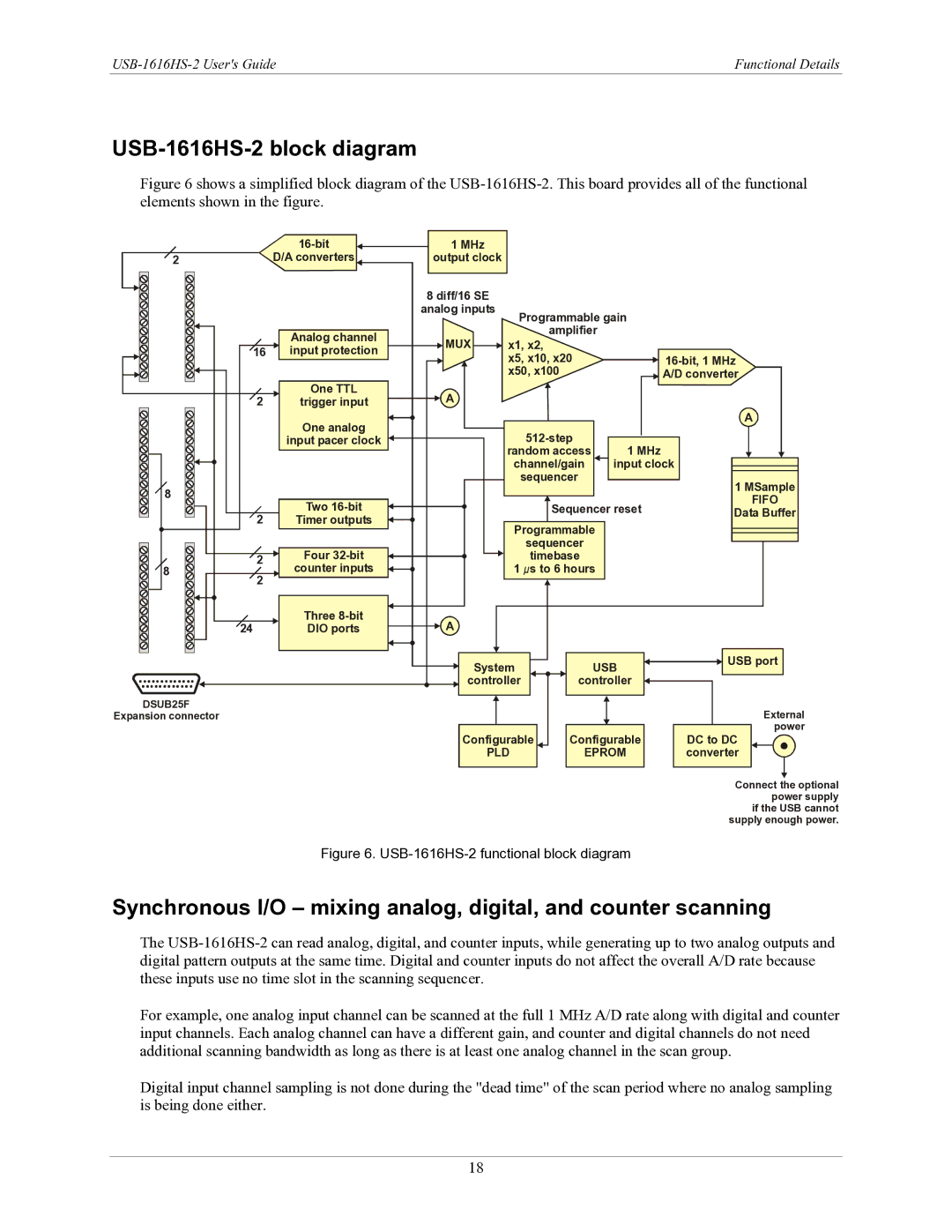
USB-1616HS-2 block diagram
USB-1616HS-2 functional block diagram
Settling time
Analog input
Analog input scanning
Example Analog channel scanning of voltage inputs
Example Analog and digital scanning, once per scan mode
Analog and digital scanning, once per scan mode example
Analog and digital scanning, once per scan mode example
Shielding
Tips for making accurate temperature measurements
Thermocouple input
Averaging
Analog output
Digital input scanning
Digital I/O
Triggering
Digital outputs and pattern generation
Hardware analog triggering
Digital triggering
Software-based triggering
Counter inputs
Stop trigger modes
Pre-triggering and post-triggering modes
Mapped channels
Totalize mode
Tips for making high-speed counter measurements 1 MHz
Counter modes
Debounce modes
Trigger after stable mode
Trigger before stable mode
Debounce mode comparisons
Debounce module Trigger before stable mode
Encoder mode
Optimal debounce time for trigger before stable mode
Representation of rotary shaft quadrature encoder
Connecting the USB-1616HS-2 to an encoder
Maximizing encoder accuracy
Timer outputs
Example Timer outputs
Timer output frequency examples
Using multiple USB-1616HS-2s per PC
Detection setpoint overview
Criteria input signal is equal to Action driven by condition
Setpoint configuration
Using the setpoint status register
Detecting on analog input, DAC, and Firstportc updates
Examples of control outputs
Detection on an analog input, timer output updates
Analog inputs with setpoints update on True and False
Using the hysteresis function
Timer output update on True and False
Using multiple inputs to control one DAC output
Detecting setpoints on a totalizing counter
FIRSTPORTC, DAC, or timer update latency
Controlling analog, digital, and timer outputs
Detection setpoint details
Firstportc
Calibrating the USB-1616HS-2
Analog input accuracy specifications
Specifications
Analog input specifications
Accuracy
Thermocouples
Analog output specifications
Analog outputs
Thermocouple TC types and accuracy Note
Digital input/output specifications
Digital input/output
Counters
Counter specifications
Input sequencer specifications
Input sequencer
Power consumption specifications Note
Power consumption
Frequency/pulse generator specifications
Frequency/pulse generators
Signal I/O connectors and pin out
External power
USB specifications
Environmental
USB-1616HS-2 screw terminal pin out single-ended connections
USB-1616HS-2 screw terminal pin out differential connections
Declaration of Conformity
USA
Mailinfo@mccdaq.com