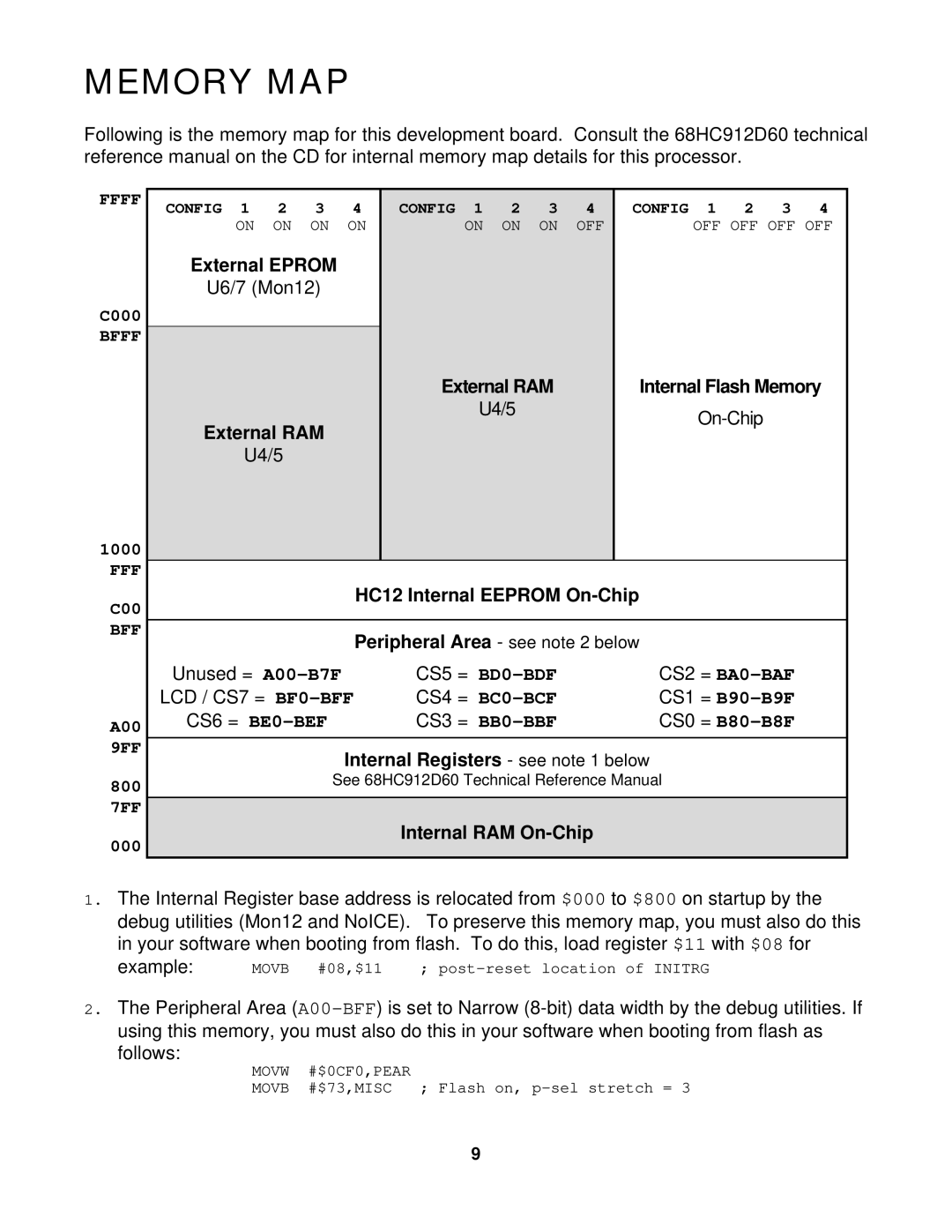
MEMORY MAP
Following is the memory map for this development board. Consult the 68HC912D60 technical reference manual on the CD for internal memory map details for this processor.
FFFF | CONFIG 1 | 2 | 3 | 4 | CONFIG 1 | 2 | 3 | 4 | CONFIG 1 2 3 4 |
| |||||||||
| ON | ON | ON | ON | ON | ON | ON | OFF | OFF OFF OFF OFF |
|
| External EPROM |
|
|
|
|
|
|
| U6/7 (Mon12) |
|
|
|
|
|
C000 |
|
|
|
|
|
|
|
BFFF |
|
|
|
|
|
| |
|
|
|
|
| External RAM | Internal Flash Memory | |
|
|
|
|
| U4/5 | ||
|
| External RAM |
|
|
| ||
|
|
|
|
|
|
| |
|
| U4/5 |
|
|
|
|
|
1000 |
|
|
|
|
|
|
|
FFF |
|
|
|
|
|
| |
C00 |
|
| HC12 Internal EEPROM |
|
| ||
|
|
|
|
|
| ||
BFF |
| Peripheral Area - see note 2 below | |||||
|
|
| |||||
|
| Unused = |
|
| CS5 = | CS2 = | |
|
| LCD / CS7 = |
|
| CS4 = | CS1 = | |
A00 |
| CS6 = |
|
| CS3 = | CS0 = | |
|
|
|
|
|
| ||
9FF | Internal Registers - see note 1 below | ||||||
|
| ||||||
800 |
| See 68HC912D60 Technical Reference Manual | |||||
|
|
|
|
|
|
| |
7FF |
|
|
|
|
|
| |
000 |
|
|
|
| Internal RAM |
|
|
|
|
|
|
|
|
| |
1.The Internal Register base address is relocated from $000 to $800 on startup by the debug utilities (Mon12 and NoICE). To preserve this memory map, you must also do this in your software when booting from flash. To do this, load register $11 with $08 for
example: | MOVB #08,$11 | ; |
2.The Peripheral Area
follows:
MOVW | #$0CF0,PEAR |
MOVB | #$73,MISC ; Flash on, |
9