Technical Specifications | Appendix A | |
|
|
|
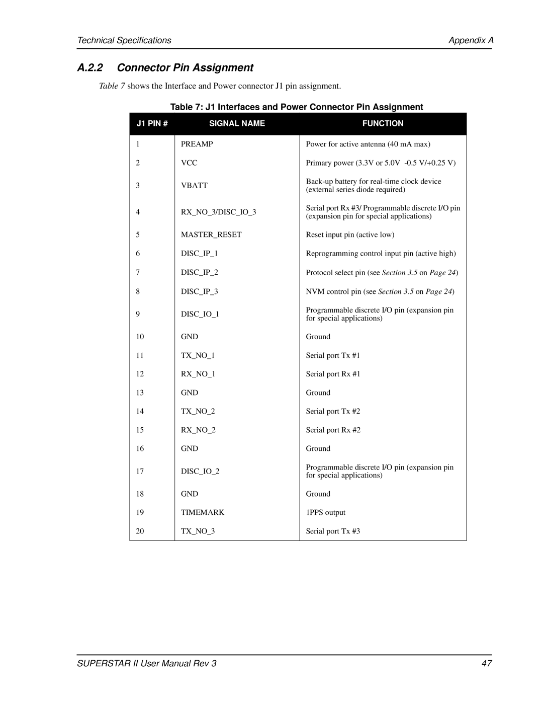
A.2.2 Connector Pin Assignment
Table 7 shows the Interface and Power connector J1 pin assignment.
Table 7: J1 Interfaces and Power Connector Pin Assignment
J1 PIN # | SIGNAL NAME | FUNCTION | |
|
|
| |
1 | PREAMP | Power for active antenna (40 mA max) | |
2 | VCC | Primary power (3.3V or 5.0V | |
3 | VBATT | ||
(external series diode required) | |||
|
| ||
4 | RX_NO_3/DISC_IO_3 | Serial port Rx #3/ Programmable discrete I/O pin | |
(expansion pin for special applications) | |||
|
| ||
5 | MASTER_RESET | Reset input pin (active low) | |
6 | DISC_IP_1 | Reprogramming control input pin (active high) | |
7 | DISC_IP_2 | Protocol select pin (see Section 3.5 on Page 24) | |
8 | DISC_IP_3 | NVM control pin (see Section 3.5 on Page 24) | |
9 | DISC_IO_1 | Programmable discrete I/O pin (expansion pin | |
for special applications) | |||
|
| ||
10 | GND | Ground | |
11 | TX_NO_1 | Serial port Tx #1 | |
12 | RX_NO_1 | Serial port Rx #1 | |
13 | GND | Ground | |
14 | TX_NO_2 | Serial port Tx #2 | |
15 | RX_NO_2 | Serial port Rx #2 | |
16 | GND | Ground | |
17 | DISC_IO_2 | Programmable discrete I/O pin (expansion pin | |
for special applications) | |||
|
| ||
18 | GND | Ground | |
19 | TIMEMARK | 1PPS output | |
20 | TX_NO_3 | Serial port Tx #3 | |
|
|
|
SUPERSTAR II User Manual Rev 3 | 47 |