KX-TC2000NZB / KX-TC2000N ZW / KX-TC2000NZF
10 TROUBLESHOOTING GUIDE
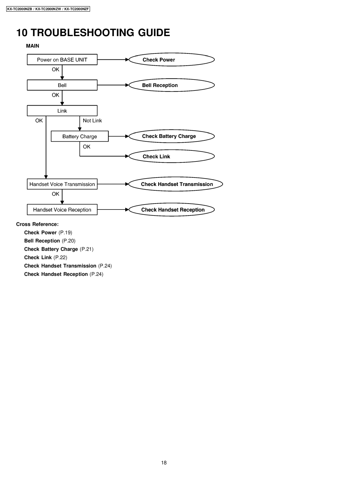
Cross Reference:
Check Power (P.19)
Bell Reception (P.20)
Check Battery Charge (P.21)
Check Link (P.22)
Check Handset Transmission (P.24)
Check Handset Reception (P.24)
18