
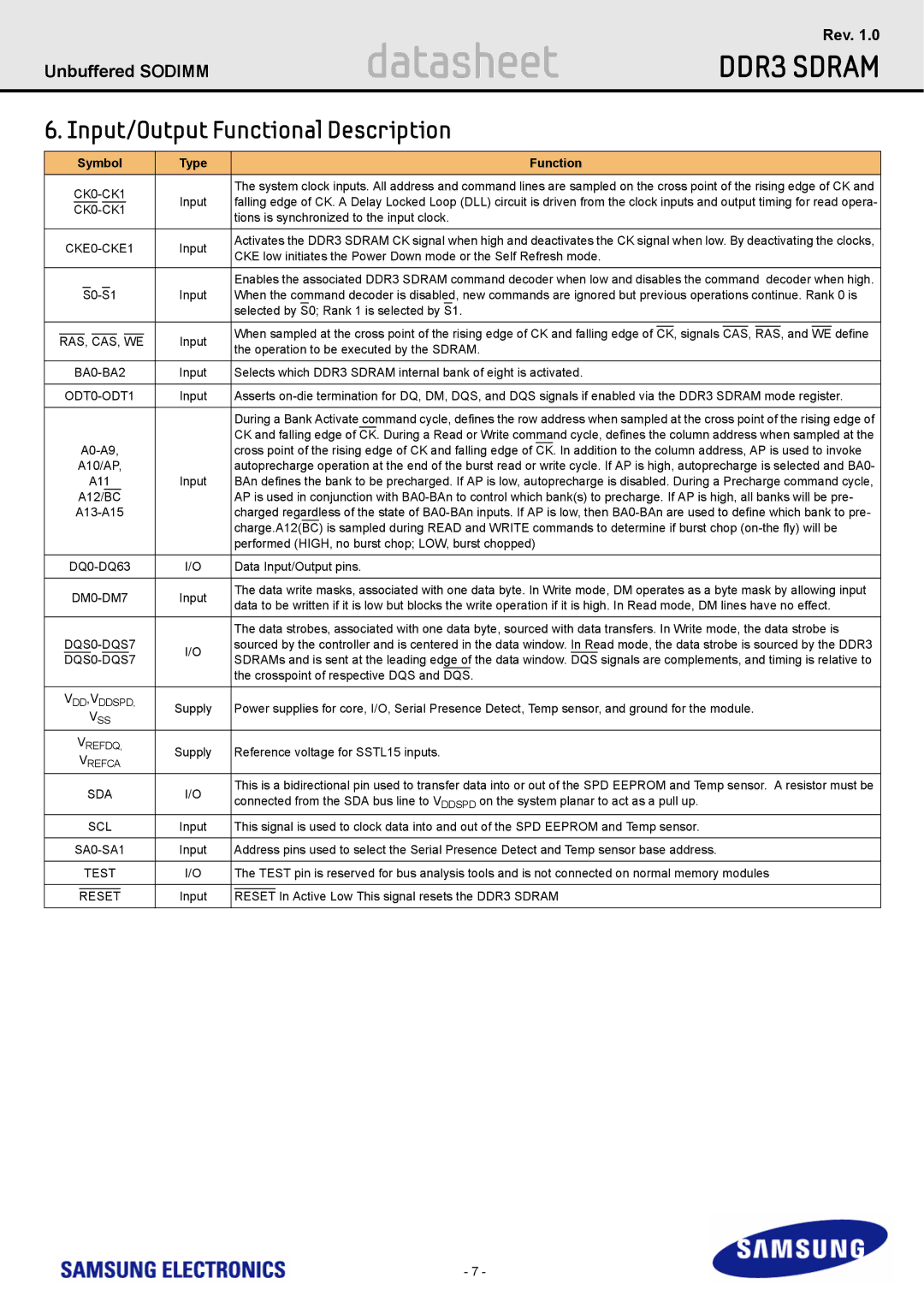
M471B1G73AH0 specifications
The Samsung M471B1G73AH0 is a high-performance DDR4 SO-DIMM memory module designed for laptops and compact systems. This specific RAM chip showcases a balance of speed, efficiency, and reliability, making it an ideal choice for both everyday users and professionals seeking enhanced system performance.One of the main features of the M471B1G73AH0 is its capacity. With 8GB of memory, it provides ample space for multitasking, allowing users to run multiple applications simultaneously without experiencing slowdowns. This is particularly beneficial for users who require a robust performance for tasks such as video editing, gaming, or running virtual machines.
The module operates at a frequency of 2400 MHz, tapping into the capabilities of DDR4 technology. This frequency ensures that data can be transferred quickly, enhancing overall system responsiveness. The DDR4 specification also brings improvements in power efficiency compared to its predecessor, DDR3, resulting in lower energy consumption and prolonged battery life in portable devices.
Another notable aspect of the M471B1G73AH0 is its latency. With a CAS latency of CL17, this module strikes a good balance between speed and response time, ensuring that data retrieval and execution are efficient, which is crucial for both applications and system processes.
Samsung’s advanced manufacturing technology is evident in this module, which employs 20nm process technology to produce high-density chips. This not only contributes to lower power consumption but also results in a smaller physical footprint, allowing for increased memory density in compact devices.
In terms of compatibility, the M471B1G73AH0 is designed to support a wide range of platforms. It adheres to the standard SO-DIMM form factor, making it compatible with most laptops and all-in-one systems. This versatility allows users to easily upgrade their existing systems for enhanced performance.
Additionally, the module includes features such as ECC (Error-Correcting Code) capabilities for certain variants, which helps in identifying and correcting memory errors, thereby increasing system reliability—an essential aspect for critical applications.
In conclusion, the Samsung M471B1G73AH0 is a robust DDR4 memory solution that delivers solid performance and reliability. With its 8GB capacity, 2400 MHz frequency, and energy-efficient design, it is suitable for a wide range of computing needs, making it a popular choice among users looking to upgrade their systems for improved efficiency and responsiveness.