Overview
Features
Sisecure
Document No Release Date Changes
Revision History
4300D-00DSR February 27 Initial release
Table of Contents
Task File Register Specification
Related Documentation
Sales and Support Part Numbering
List of Figures
List of Tables
Idle Immediate 95h, E1h
Part Numbering Nomenclature
Physical Dimensions
Physical Specifications
Pin Locations
System Power Requirements
Product Specifications
System Performance
Reliability
SiliconDrive Part# Capacity Service Life GB Written per Day
Operational Life Span
Years 402.9GB SSD-D004G-4300
Environmental Specifications
Product Capacity Specifications
Product Capacity Number Bytes Sectors Cylinders Heads Track
Pin Assignments
Electrical Specification
Pin
Ultra DMA
Signal Name Pins Type Description
Signal Descriptions
Data Inputs/Outputs. This is the 8-bit or
Disk Active/Slave Present. This open
Transfers between the host and device
DMA Request. This signal is used for DMA
Ground. The device ground signal
This signal is a DMA request that is used
Interrupt Request. This signal is an active
For DMA data transfers between the host
When Udma mode DMA write is active
Channel Ready. The signal is negated
When Udma mode DMA read is active
Device I/O Read. This is the read strobe
Symbol Parameter Minimum Maximum Units
Device Power Supply. The device power
Absolute Maximum Ratings
Symbol Parameter 5V ± 10% Units Minimum Maximum
DC Characteristics
True IDE PIO Mode Read/Write Access Timing Diagram
True IDE PIO Mode Read/Write Access Timing
True IDE PIO Mode Read/Write Access Timing
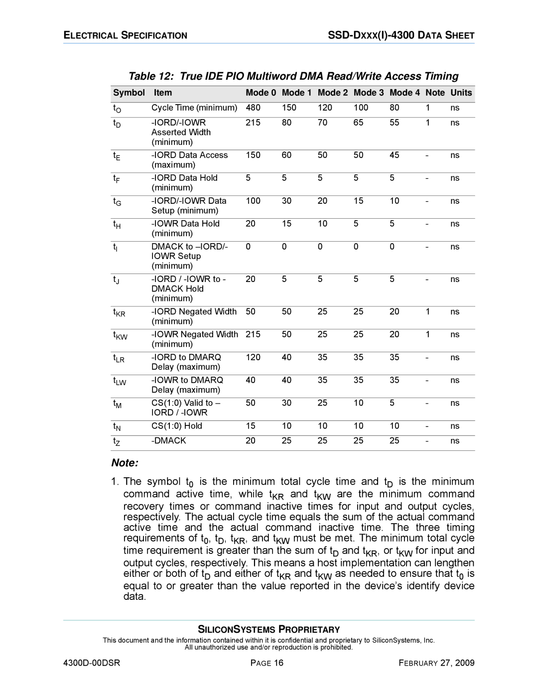
True IDE PIO Multiword DMA Read/Write Access Timing
Symbol Mode 0 Mode Mode 3 Mode 4 Note Units
True IDE PIO Multiword DMA Read/Write Access Timing
Initiating a Udma Data-In Burst
Ultra DMA Data Burst Timing Requirements
Sustained Udma Data-In Burst
Device Terminating a Udma Data-In Burst
Host Terminating a Udma Data-In Burst
Initiating a Udma Data-Out Burst
Device Pausing a Udma Data-Out Burst
Host Terminating a Udma Data-Out Burst
Udma Data Burst Timing Requirements
Device Terminating a Udma Data-Out Burst
Min Max Min. Max
Time from Strobe edge to ns
ATA and True IDE Register Decoding
Task File Register Specification
CS0# CS1# DA02 DA01 DA00
ATA Registers
Error Register
Operation
Feature Register
Read/Write
Byte
Sector Count Register
Read/Write Sector Count Default Value
Read/Write
Sector Number Register
Logical Block Number bits A07-A00 LBA Addressing
Low
Cylinder Low Register
Logical Block Number bits A15-A08 LBA Addressing
Logical Block Number bits A23-A16 LBA Addressing
Cylinder High Register
LBA27 LBA26 LBA25 LBA24
Drive/Head Register
Status Register
Drive Write Fault DWF. Always set to
Corrected Data CORR. Always set to
Operation Read/Write ATA Command Code
Command Register
Alternate Status Register
Write
Device Control Register
NIEN
Device Address Register
Read/Write NWTG NHS3 NHS2 NHS1 NHS0 NDS1 NDS0 Default Value
ATA Command Block and Set Description
ATA Command Block and SET Description
ATA Command Set
Class Command Name Registers Used Code
ATA Command Set
Check Power Mode 98h, E5h
Check Power Mode 98h, E5h
Register
Executive Drive Diagnostic 90h
Executive Drive Diagnostic 90h
Format Track 50h
Drive Head Number LBA27-24 Command 50h
Format Track 50h
Identify Drive ECh
Identify Drive ECh
Identify Drive Drive Attribute Data
Word Data Default Bytes Data Description Address
Identify Drive Drive Attribute Data
Identify Drive Drive Attribute Data
Idle 97h, E3h
Idle 97h, E3h
Idle Immediate 95h, E1h
Idle Immediate 95h, E1h
Initialize Drive Parameters 91h
Initialize Drive Parameters 91h
Recalibrate 1Xh
Drive Command 1Xh
Recalibrate 1Xh
Read Buffer E4h
Read Buffer E4h
Read DMA C8h
Drive Head Number LBA27-24 Command C8h
Read DMA C8h
Read Multiple C4h
Drive Head Number LBA27-24 Command C4h
Read Multiple C4h
Read Sector 20h, 21h
Drive Head Number LBA27-24 Command 20h or 21h
Read Sector 20h, 21h
Read Long Sectors 22h, 23h
Drive Head Number LBA27-24 Command 22h or 23h
Read Long Sectors 22h, 23h
Read Verify Sectors 40h, 41h
Drive Head Number LBA27-24 Command 40h or 41h
Read Verify Sectors 40h, 41h
Seek 7Xh
Drive Head Number LBA27-24 Command 7Xh
Seek 7Xh
Set Features EFh
Set Features EFh
Set Features’ Attributes
Feature Operation
Set Multiple Mode C6h
Set Multiple Mode C6h
Set Sleep Mode 99h, E6h
Set Sleep Mode 99h, E6h
Standby 96h, E2h
Standby 96h, E2h
Standby Immediate 94h, E0h
Standby Immediate 94h, E0h
Write Buffer E8h
Write Buffer E8h
Write DMA CAh
Drive Head NumberLBA27-24 Command CAh
Write DMA CAh
Write Multiple C5h
Drive Head NumberLBA27-24 Command C5h
Write Multiple C5h
Write Sectors 30h, 31h
Drive Head Number LBA27-24 Command 30h or 31h
Write Sectors 30h, 31h
Write Long Sectors 32h, 33h
Drive Head Number LBA27-24 Command 32h or 33h
Write Long Sectors 32h, 33h
Erase Sectors C0h
Drive Head Number LBA27-24 Command C0h
Erase Sectors C0h
Extended Error Codes Description
Extended Error Codes
Request Sense 03h
Request Sense 03h
Translate Sector 87h
Drive Head Number LBA27-24 Command 87h
Translate Sector 87h
Wear-Level F5h
Wear-Level F5h
Write Multiple w/o Erase CDh
Drive Head Number LBA27-24 Command CDh
Write Multiple w/o Erase CDh
Write Sectors w/o Erase 38h
Drive Head Number LBA27-24 Command 38h
Write Sectors w/o Erase 38h
Write Verify 3Ch
Drive Head Number LBA27-24 Command 3Ch
Write Verify 3Ch
Part Numbering
Sales and Support
Part Numbering Nomenclature
Part Numbers
Front Label Lot Code Information
Standard Back Label with
Related Documentation
Related Documentation