| |
MEMO | MEMO |
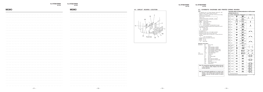
CIRCUIT BOARDS LOCATION |
KL-W7000/W9000
KL-W7000/W9000
4-3. SCHEMATIC DIAGRAMS AND PRINTED WIRING BOARDS
| C | |
TB |
| |
HB |
| |
| K | |
TA |
| |
| U | |
| BB | |
HA | A | |
G | ||
Power block | ||
| GA |
Note:
•All capacitors are in µF unless otherwise noted. (pF: µµF) Capacitors without voltage indication are all 50 V.
•Indication of resistance, which does not have one for rating electrical power, is as follows.
Pitch: 5 mm
Rating electrical power 1/4 W (CHIP : 1/10 W)
•All resistors are in ohms.
•f : nonflammable resistor.
•ì : fusible resistor.
•¢ : internal component.
•p : panel designation, and adjustment for repair.
•All variable and adjustable resistors have characteristic curve B, unless otherwise noted.
•e :
•E :
•All voltages are in V.
•Readings are taken with a 10 M digital multimeter.
•Readings are taken with a
•Voltage variations may be noted due to normal production tolerances.
*: Can not be measured.
•Circled numbers are waveform references.
•s : B + bus.
•S : B – bus.
•m : Signal path.
Reference information
RESISTOR | : RN | METAL FILM |
| : RC | SOLID |
| : FPRD | NONFLAMMABLE CARBON |
| : FUSE | NONFLAMMABLE FUSIBLE |
| : RW | NONFLAMMABLE WIREWOUND |
| : RS | NONFLAMMABLE METAL OXIDE |
| : RB | NONFLAMMABLE CEMENT |
COIL | : | MICRO INDUCTOR |
CAPACITOR | : TA | TANTALUM |
| : PS | STYROL |
| : PP | POLYPROPYLENE |
| : PT | MYLAR |
| : MPS | METALIZED POLYESTER |
| : MPP | METALIZED POLYPROPYLENE |
| : ALB | BIPOLAR |
| : ALT | HIGH TEMPERATURE |
| : ALR | HIGH RIPPLE |
Note: The components identified by shading and mark
Áare critical for safety. Replace only with part number specified.
Note: Les composants identifiés per un tramé et une marque Á sont critiques pour la sécurité. Ne les remplacer que par une pièce portant le numéro spécifié.
Terminal name of semiconductors in silk screen printed circuit (*)
| Device Printed symbol Terminal name |
| Circuit | |||
1 | Transistor | Collector |
|
| ||
Base | Emitter |
|
| |||
|
|
|
| |||
2 | Transistor | Collector |
|
| ||
Base | Emitter |
|
| |||
|
|
|
| |||
3 | Diode | Cathode |
|
|
| |
| Anode |
|
| |||
|
|
|
|
| ||
4 |
| Cathode |
|
| ||
Diode | Anode | (NC) |
|
| ||
|
|
|
| |||
5 |
| Cathode |
|
| ||
Diode | Anode | (NC) |
|
| ||
|
|
|
| |||
6 |
| Common |
|
| ||
Diode | Anode | Cathode |
|
| ||
|
|
|
| |||
7 | Diode | Common |
|
| ||
Anode | Cathode |
|
| |||
|
|
|
| |||
8 |
| Common |
|
| ||
Diode | Anode | Anode |
|
| ||
|
|
|
| |||
9 | Diode | Common |
|
| ||
Anode | Anode |
|
| |||
|
|
|
| |||
0 Diode | Common |
|
| |||
Cathode | Cathode |
|
| |||
|
|
|
| |||
!Á | Diode | Common |
|
| ||
Cathode | Cathode |
|
| |||
|
|
|
| |||
!ª | Transistor | Drain | Source |
|
| |
(FET) | Gate | D | D | |||
| ||||||
|
|
| G |
| G | |
!£ | Transistor | Drain | Source | S | S | |
(FET) | Gate |
|
| |||
|
|
| ||||
| Transistor | Source | D |
| D |
!¢ |
|
|
| ||
(FET) | Drain |
| G | G | |
Gate | S |
| S | ||
|
|
|
|
!° |
|
| Emitter |
|
| ||
Transistor |
| Collector |
|
| |||
|
|
| Base |
|
| ||
|
| C2 B1 E1 | C1 | C2 | |||
!¤ | Transistor | B1 | B2 | ||||
E2 B2 C1 | |||||||
|
| E1 | E2 | ||||
|
|
|
|
| |||
!¦ | Transistor | C1 B2 E2 |
|
| |||
E1 B1 C2 | C1 | C2 | |||||
|
|
|
| ||||
|
|
|
|
| B1 | B2 | |
!¥ | Transistor | C1 B2 E2 | E1 | E2 | |||
E1 B1 C2 |
|
| |||||
|
|
|
| ||||
|
|
|
|
| E1 | E2 | |
!» | Transistor | C1 B2 E2 | B1 | B2 | |||
E1 B1 C2 | |||||||
|
| C1 | C2 | ||||
|
|
|
|
| |||
|
|
|
|
| C1(B2) | C2 | |
@¼ | Transistor | E2 | B1 E1 | B1 |
| ||
C2 |
| C1(B2) |
| ||||
|
|
| E2 | E2 | |||
|
|
|
|
| |||
|
|
| (B2) |
| E1(B2) | E2 | |
@Á | Transistor | B1 E1 | E2 | B1 |
| ||
C1 |
| C2 |
| ||||
|
|
| C1 | C2 | |||
|
|
|
|
| |||
|
|
| (B2) |
| E1(B2) | C2 | |
@ª | Transistor | E2 E1 B1 | B1 |
| |||
|
|
|
| ||||
|
| C2 |
| C1 | C1 | C2 | |
|
|
|
|
| |||
–Discrete semiconductot
(Chip semiconductors that are not actually used are included.) | Ver.1.4 |
|
– 51 – | – 52 – | – 53 – | – 54 – |