Manuals
/
Sony
/
Home Audio
/
Stereo System
Sony
MDS-JE530
service manual
35, Note on Printed Wiring Board, Note on Schematic Diagram
Models:
MDS-JE530
1
33
64
64
Download
64 pages
44.38 Kb
30
31
32
33
34
35
36
37
Specification
Parts list
MDS-JE530 SECTION DIAGRAMS
CD Error Rate Check
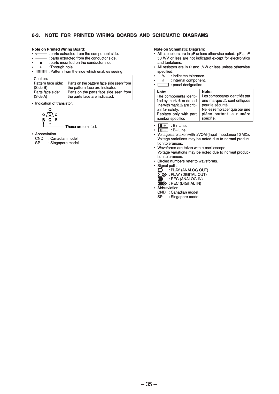
Note on Printed Wiring Board
Section Disassembly
Checking Procedure
Section Electrical Adjustments
Setting The Test Mode
Precautions For Adjustments
Page 33
Image 33
Page 32
Page 34
Page 33
Image 33
Page 32
Page 34
Contents
SERVICE MANUAL
SPECIFICATIONS
Supplied accessories
MDS-JE530
– 2 –
SELF-DIAGNOSISFUNCTION
Table of Error Codes
Items of Error History Mode Items and Contents
– 3 –
Selecting the Test Mode
6.DIAGRAMS
TABLE OF CONTENTS
DISASSEMBLY
ELECTRICAL ADJUSTMENTS
Notes on chip component replacement
Flexible Circuit Board Repairing
– 5 –
ADVARSEL
JIG FOR CHECKING BD BOARD WAVEFORM
– 6 –
– 7 –
Record Precedure
Display Precedure
– 8 –
CHECKS PRIOR TO PARTS REPLACEMENT AND ADJUSTMENTS
RETRY CAUSE DISPLAY MODE
– 9 –
Precedure
Fig. 1 Reading the Test Mode Display
– 10 –
Hexadecimal nBinary Conversion Table
Reading the Display
– 11 –
SECTION GENERAL
LOCATION OF CONTROLS
This section is extracted from instruction manual
Page
– 13 –
SECTION DISASSEMBLY
CASE
FRONT PANEL SECTION
– 14 –
MAIN BOARD
MECHANISM DECK SECTTION MDM-5D
– 15 –
SLIDER CAM
BASE UNIT MBU-5D,BD BOARD
SW BOARD, LOADING MOTOR M103
– 16 –
2. SETTING THE TEST MODE
1. PRECAUTIONS FOR USE OF TEST MODE
SECTION TEST MODE
– 17 –
5. SELECTING THE TEST MODE
– 18 –
– 19 –
5-1.Operating the Continuous Playback Mode
5-3. Non-VolatileMemory Mode EEP MODE
– 20 –
6. FUNCTIONS OF OTHER BUTTONS
7. TEST MODE DISPLAYS
MEANINGS OF OTHER DISPLAYS
– 21 –
SECTION ELECTRICAL ADJUSTMENTS
1.PARTS REPLACEMENT AND ADJUSTMENT
– 22 –
4. PRECAUTIONS FOR ADJUSTMENTS
2. PRECAUTIONS FOR CHECKING LASER DIODE EMISSION
Laser power meter
– 23 –
6-2.Laser Power Check
Checking Procedure
Specification
– 24 –
CD Error Rate Check
6-5.C PLAY Checking MO Error Rate Check
– 25 –
6-4.Focus Bias Check
9. TEMPERATURE COMPENSATION OFFSET ADJUSTMENT
7. INITIAL SETTING OF ADJUSTMENT VALUE
10. LASER POWER ADJUSTMENT
Setting Procedure
– 27 –
11. TRAVERSE ADJUSTMENT
Specification
Adjusting Procedure
12.FOCUS BIAS ADJUSTMENT
– 28 –
Adjusting Procedure
15.AUTO GAIN CONTROL OUTPUT LEVEL ADJUSTMENT
13.ERROR RATE CHECK
13-1.CD Error Rate Check
13-2.MO Error Rate Check
– 30 –
Adjustment Location
– BD BOARDSide A –
– BD BOARDSide B –
6-1.BLOCK DIAGRAM – MD SERVO Section –
MDS-JE530 SECTION DIAGRAMS
– 31 –
– 32 –
MDS-JE530
6-2.BLOCK DIAGRAM – MAIN Section –
– 33 –
– 34 –
– 35 –
Note on Printed Wiring Board
Note on Schematic Diagram
• Circuit Boards Location
– 36 –
– 38 –
6-4.PRINTED WIRING BOARD – BD Board –
•See page 36 for Circuit Boards Location
•Semiconductor Location
– 39 –
– 40 –
MDS-JE530
– 41 –
6-6.SCHEMATIC DIAGRAM – BD Board 2/2 – See•
– 42 –
MDS-JE530
6-8.PRINTED WIRING BOARD – SW Board –
6-7.SCHEMATIC DIAGRAM – SW Board –
– 43 –
– 44 –
– 45 –
6-9.PRINTED WIRING BOARD – MAIN Board – See•
– 46 –
page 36 for Circuit Boards Location
– 48 –
– 47 –
MDS-JE530
Page Page 41 Page
– 49 –
– 50 –
MDS-JE530
– 52 –
– 51 –
MDS-JE530
• Semiconductor Location
– 54 –
– 53 –
MDS-JE530
Page 47 Page
– 55 –
•IC Block Diagrams – BD Board –
– 56 –
IC101
IC310
– 57 –
M5293L
IC431
6-14.IC PIN FUNCTION DESCRIPTION
– 58 –
•BD BOARD IC121 CXD2656R
– 59 –
– 60 –
– 61 –
•MAIN BOARD IC501 M30624MG-207FPSYSTEM CONTROLLER
– 62 –
– 63 –
– 64 –
SECTION EXPLODED VIEWS
– 65 –
1CHASSIS SECTION
66 61 61
2FRONT PANEL SECTION 61 64 61 63 61
51 53
59 54 52
3MECHANISM SECTION MDM-5D 213 207
– 67 –
202 201
223 207
4BASE UNIT SECTION MBU-5D 252
– 68 –
263 270
254 253
– 69 –
SECTION ELECTRICAL PARTS LIST
– 70 –
DISPLAY
KEY SW
– 71 –
DISPLAY
MAIN
– 72 –
KEY SW
MAIN
– 73 –
MAIN
– 74 –
POWER SW
– 75 –
MAIN
– 76 –
MDS-JE530
Sony Corporation
9-928-824-11
Top
Page
Image
Contents