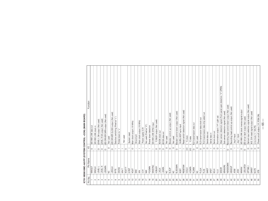
•IC701 M30610MC-A01FP (SYSTEM CONTROL ∝CON) (MAIN BOARD)
Pin No. | Pin Name | I/O | Function | |
1 | WMOUT | O | MD WM LINK data out | |
|
|
|
| |
2 | WMCLK | I | MD WM LINK clock in | |
|
|
|
| |
3 | O | |||
|
|
|
| |
4 | O | |||
|
|
|
| |
5 | LEDDATA | O | LED DRIVER DATA output (Not used) | |
|
|
|
| |
6 | NC | O | Not used | |
|
|
|
| |
7 | LEDCLK | O | LED DRIVER CLOCK output (Not used) | |
|
|
|
| |
8 | BYTE | I | Data bus switching (Fixed at “L”) | |
|
|
|
| |
9 | CNVSS | I | Pulled down to “L” | |
|
|
|
| |
10 | I | Not used | ||
|
|
| ||
11 | O | |||
| ||||
|
|
|
| |
12 | S.RST | I | System reset | |
|
|
|
| |
13 | XOUT | O | Main clock output (10 MHz) | |
|
|
|
| |
14 | GND | – | Ground pin | |
|
|
|
| |
15 | XIN | I | Main clock output (10 MHz) | |
|
|
|
| |
16 | 3.3V | – | Power supply 3.3V | |
|
|
|
| |
17 | NMI | I | Not used (Fixed at “H”) | |
|
|
|
| |
18 | P.DOWN | I | Power down detection | |
|
|
|
| |
19 | WMSYNC | I | MD WM LINK SYNC input | |
|
|
|
| |
20 | IICBUSY | O | I2C BUSY output (Not used) | |
21 | L3CLK | O | AD/DA clock out | |
|
|
|
| |
22 | L3DATA | O | AD/DA data out | |
|
|
|
| |
23 | NC | O | Not used | |
|
|
|
| |
24 | ELEUP | O | Elevator control up output (Not used) | |
|
|
|
| |
25 | NC | O | Not used | |
|
|
|
| |
26 | ELEDOWN | O | Elevator control down output (Not used) | |
|
|
|
| |
27 | SQSY | I | SUBQ, ADIP sync input | |
|
|
|
| |
28 | RESETSW | I | Reset switch detection signal (Not used) | |
|
|
|
| |
29 | IICCLK | I/O | I2C clock | |
|
|
|
| |
30 | IICDATA | I/O | I2C data | |
31 | FLDATA | O | FLD transmission data out | |
|
|
|
| |
32 | NC | O | Not used | |
|
|
|
| |
33 | FLCLK | O | FLD transmission data clock out | |
|
|
|
| |
34 | FLCS | O | FLD transmission data chip select out | |
|
|
|
| |
35 | SWDT | O | Serial data out | |
|
|
|
| |
36 | SRDT | I | Serial data in | |
|
|
|
| |
37 | SCLK | O | Serial clock out | |
|
|
|
| |
38 | ILLU | O | Illumination output (“H”:Light up) | |
|
|
|
| |
39 | SESOR | I | Main sensor detection signal (Front panel open detection “H”:OPEN) | |
|
|
|
| |
40 | SENSOR2 | I | Sub sensor detection signal (Not used) | |
|
|
|
| |
41 | HEADDOWN | O | Recording head control down output (Not used) | |
|
|
|
| |
42 | HEADUP | O | Recording head control up output (Not used) | |
|
|
|
| |
43 | JOG0 | I | Jog 0 input | |
|
|
|
| |
44 | JOG1 | I | Jog 1 input | |
|
|
|
| |
45 | WMINV | O | MD WM LINK clock inverse signal output | |
|
|
|
| |
46 | LEDLATCH | O | LED driver latch output (Not used) | |
|
|
|
| |
47 | OPTSEL1 | O | Optical input selection signal output (Not used) | |
|
|
|
| |
48 | DARST | O | A/D, D/A reset signal output (Not used) | |
|
|
|
| |
49 | MUTE | O | Line mute (“L”:MUTE) | |
|
|
|
| |
50 | STB | O | Power on/off output (“H”:POW ON) | |
|
|
|
|
– 65 –