NW-MS6
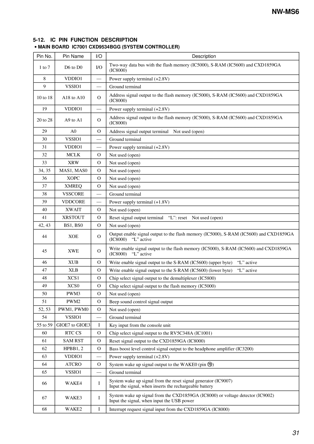
5-12. IC PIN FUNCTION DESCRIPTION
•MAIN BOARD IC7001 CXD9534BGG (SYSTEM CONTROLLER)
Pin No. | Pin Name | I/O |
| Description |
|
|
|
|
| ||
1 to 7 | D6 to D0 | I/O | |||
(IC8000) |
|
| |||
|
|
|
|
| |
|
|
|
|
| |
8 | VDDIO1 | — | Power supply terminal (+2.8V) |
| |
|
|
|
|
| |
9 | VSSIO1 | — | Ground terminal |
| |
|
|
|
| ||
10 to 18 | A18 to A10 | O | Address signal output to the flash memory (IC5000), | ||
(IC8000) |
|
| |||
|
|
|
|
| |
|
|
|
|
| |
19 | VDDIO1 | — | Power supply terminal (+2.8V) |
| |
|
|
|
| ||
20 to 28 | A9 to A1 | O | Address signal output to the flash memory (IC5000), | ||
(IC8000) |
|
| |||
|
|
|
|
| |
|
|
|
|
| |
29 | A0 | O | Address signal output terminal Not used (open) |
| |
|
|
|
|
| |
30 | VSSIO1 | — | Ground terminal |
| |
|
|
|
|
| |
31 | VDDIO1 | — | Power supply terminal (+2.8V) |
| |
|
|
|
|
| |
32 | MCLK | O | Not used (open) |
| |
|
|
|
|
| |
33 | XRW | O | Not used (open) |
| |
|
|
|
|
| |
34, 35 | MAS1, MAS0 | O | Not used (open) |
| |
|
|
|
|
| |
36 | XOPC | O | Not used (open) |
| |
|
|
|
|
| |
37 | XMREQ | O | Not used (open) |
| |
|
|
|
|
| |
38 | VSSCORE | — | Ground terminal |
| |
|
|
|
|
| |
39 | VDDCORE | — | Power supply terminal (+1.8V) |
| |
|
|
|
|
| |
40 | XWAIT | O | Not used (open) |
| |
|
|
|
|
| |
41 | XRSTOUT | O | Reset signal output terminal “L”: reset Not used (open) |
| |
|
|
|
|
| |
42, 43 | BS1, BS0 | O | Not used (open) |
| |
|
|
|
| ||
44 | XOE | O | Output enable signal output to the flash memory (IC5000), | ||
(IC8000) | “L” active |
| |||
|
|
|
| ||
|
|
|
| ||
45 | XWE | O | Write enable signal output to the flash memory (IC5000), | ||
(IC8000) | “L” active |
| |||
|
|
|
| ||
|
|
|
|
| |
46 | XUB | O | Write enable signal output to the | “L” active | |
|
|
|
|
| |
47 | XLB | O | Write enable signal output to the | “L” active | |
|
|
|
|
| |
48 | XCS1 | O | Chip select signal output to the demultiplexer (IC5800) |
| |
|
|
|
|
| |
49 | XCS0 | O | Chip select signal output to the flash memory (IC5000) |
| |
|
|
|
|
| |
50 | PWM3 | O | Not used (open) |
| |
|
|
|
|
| |
51 | PWM2 | O | Beep sound control signal output |
| |
|
|
|
|
| |
52, 53 | PWM1, PWM0 | O | Not used (open) |
| |
|
|
|
|
| |
54 | VSSIO1 | — | Ground terminal |
| |
|
|
|
|
| |
55 to 59 | GIOE7 to GIOE3 | I | Key input from the console unit |
| |
|
|
|
|
| |
60 | RTC CS | O | Chip select signal output to the RV5C348A (IC1001) |
| |
|
|
|
|
| |
61 | SAM RST | O | Reset signal output to the CXD1859GA (IC8000) |
| |
|
|
|
| ||
62 | HPBB1, 2 | O | Bass boost level control signal output to the headphone amplifier (IC3200) | ||
|
|
|
|
| |
63 | VDDIO1 | — | Power supply terminal (+2.8V) |
| |
|
|
|
|
| |
64 | ATCRO | O | System wake up signal output to the WAKE0 (pin u;) |
| |
|
|
|
|
| |
65 | VSSIO1 | — | Ground terminal |
| |
|
|
|
|
| |
66 | WAKE4 | I | System wake up signal from the reset signal generator (IC9007) |
| |
Input the signal, when inserts the rechargeable battery |
| ||||
|
|
|
| ||
|
|
|
| ||
67 | WAKE3 | I | System wake up signal from the CXD1859GA (IC8000) or voltage detector (IC9002) | ||
Input the signal, when input the USB power |
| ||||
|
|
|
| ||
|
|
|
|
| |
68 | WAKE2 | I | Interrupt request signal input from the CXD1859GA (IC8000) |
| |
|
|
|
|
|
|
31