NW-MS6
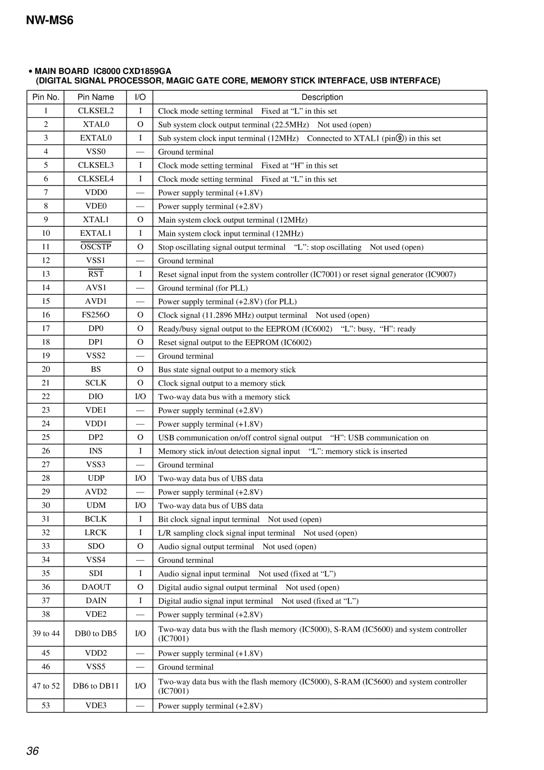
•MAIN BOARD IC8000 CXD1859GA
(DIGITAL SIGNAL PROCESSOR, MAGIC GATE CORE, MEMORY STICK INTERFACE, USB INTERFACE)
Pin No. |
| Pin Name | I/O |
|
|
| Description | |||
|
|
|
|
|
|
|
| |||
1 |
| CLKSEL2 | I | Clock mode setting terminal | Fixed at “L” in this set | |||||
|
|
|
|
|
|
|
| |||
2 |
| XTAL0 | O | Sub system clock output terminal (22.5MHz) | Not used (open) | |||||
|
|
|
|
|
|
|
| |||
3 |
| EXTAL0 | I | Sub system clock input terminal (12MHz) | Connected to XTAL1 (pin9) in this set | |||||
|
|
|
|
|
|
|
|
|
|
|
4 |
| VSS0 | — | Ground terminal |
|
|
|
| ||
|
|
|
|
|
|
|
| |||
5 |
| CLKSEL3 | I | Clock mode setting terminal | Fixed at “H” in this set | |||||
|
|
|
|
|
|
|
| |||
6 |
| CLKSEL4 | I | Clock mode setting terminal | Fixed at “L” in this set | |||||
|
|
|
|
|
|
|
|
|
| |
7 |
| VDD0 | — | Power supply terminal (+1.8V) |
|
|
| |||
|
|
|
|
|
|
|
|
|
| |
8 |
| VDE0 | — | Power supply terminal (+2.8V) |
|
|
| |||
|
|
|
|
|
|
|
| |||
9 |
| XTAL1 | O | Main system clock output terminal (12MHz) |
| |||||
|
|
|
|
|
|
|
| |||
10 |
| EXTAL1 | I | Main system clock input terminal (12MHz) |
| |||||
|
|
|
|
|
|
|
| |||
11 |
| OSCSTP | O | Stop oscillating signal output terminal | “L”: stop oscillating Not used (open) | |||||
|
|
|
|
|
|
|
|
|
|
|
12 |
| VSS1 | — | Ground terminal |
|
|
|
| ||
|
|
|
|
|
|
| ||||
13 |
|
| RST | I | Reset signal input from the system controller (IC7001) or reset signal generator (IC9007) | |||||
|
|
|
|
|
|
|
|
|
|
|
14 |
| AVS1 | — | Ground terminal (for PLL) |
|
|
|
| ||
|
|
|
|
|
|
| ||||
15 |
| AVD1 | — | Power supply terminal (+2.8V) (for PLL) |
|
| ||||
|
|
|
|
|
| |||||
16 |
| FS256O | O | Clock signal (11.2896 MHz) output terminal | Not used (open) | |||||
|
|
|
|
|
| |||||
17 |
|
| DP0 | O | Ready/busy signal output to the EEPROM (IC6002) “L”: busy, “H”: ready | |||||
|
|
|
|
|
|
| ||||
18 |
|
| DP1 | O | Reset signal output to the EEPROM (IC6002) |
| ||||
|
|
|
|
|
|
|
|
| ||
19 |
| VSS2 | — | Ground terminal |
|
|
|
| ||
|
|
|
|
|
|
|
| |||
20 |
|
| BS | O | Bus state signal output to a memory stick |
|
| |||
|
|
|
|
|
|
|
| |||
21 |
| SCLK | O | Clock signal output to a memory stick |
|
|
| |||
|
|
|
|
|
|
|
| |||
22 |
|
| DIO | I/O |
|
| ||||
|
|
|
|
|
|
|
| |||
23 |
| VDE1 | — | Power supply terminal (+2.8V) |
|
|
| |||
|
|
|
|
|
|
|
| |||
24 |
| VDD1 | — | Power supply terminal (+1.8V) |
|
|
| |||
|
|
|
|
|
| |||||
25 |
|
| DP2 | O | USB communication on/off control signal output “H”: USB communication on | |||||
|
|
|
|
|
|
| ||||
26 |
|
| INS | I | Memory stick in/out detection signal input | “L”: memory stick is inserted | ||||
|
|
|
|
|
|
|
|
| ||
27 |
| VSS3 | — | Ground terminal |
|
|
|
| ||
|
|
|
|
|
|
|
| |||
28 |
| UDP | I/O |
|
|
| ||||
|
|
|
|
|
|
|
| |||
29 |
| AVD2 | — | Power supply terminal (+2.8V) |
|
|
| |||
|
|
|
|
|
|
|
| |||
30 |
| UDM | I/O |
|
|
| ||||
|
|
|
|
| ||||||
31 |
| BCLK | I | Bit clock signal input terminal Not used (open) | ||||||
|
|
|
|
|
| |||||
32 |
| LRCK | I | L/R sampling clock signal input terminal | Not used (open) | |||||
|
|
|
|
|
| |||||
33 |
| SDO | O | Audio signal output terminal | Not used (open) | |||||
|
|
|
|
|
|
|
|
| ||
34 |
| VSS4 | — | Ground terminal |
|
|
|
| ||
|
|
|
|
|
|
| ||||
35 |
|
| SDI | I | Audio signal input terminal | Not used (fixed at “L”) | ||||
|
|
|
|
|
| |||||
36 |
| DAOUT | O | Digital audio signal output terminal | Not used (open) | |||||
|
|
|
|
| ||||||
37 |
| DAIN | I | Digital audio signal input terminal Not used (fixed at “L”) | ||||||
|
|
|
|
|
|
|
| |||
38 |
| VDE2 | — | Power supply terminal (+2.8V) |
|
|
| |||
|
|
|
|
|
|
| ||||
39 to 44 |
| DB0 to DB5 | I/O | |||||||
| (IC7001) |
|
|
|
| |||||
|
|
|
|
|
|
|
|
|
| |
|
|
|
|
|
|
|
| |||
45 |
| VDD2 | — | Power supply terminal (+1.8V) |
|
|
| |||
|
|
|
|
|
|
|
|
| ||
46 |
| VSS5 | — | Ground terminal |
|
|
|
| ||
|
|
|
|
|
|
| ||||
47 to 52 |
| DB6 to DB11 | I/O | |||||||
| (IC7001) |
|
|
|
| |||||
|
|
|
|
|
|
|
|
|
| |
|
|
|
|
|
|
|
| |||
53 |
| VDE3 | — | Power supply terminal (+2.8V) |
|
|
| |||
|
|
|
|
|
|
|
|
|
|
|
36