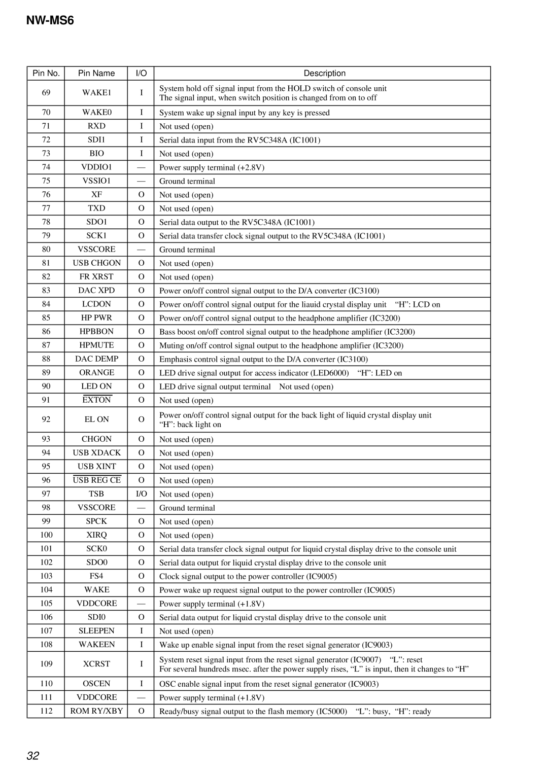
NW-MS6
Pin No. |
| Pin Name | I/O | Description |
|
| |
|
|
|
|
|
|
| |
69 |
| WAKE1 | I | System hold off signal input from the HOLD switch of console unit |
| ||
| The signal input, when switch position is changed from on to off |
| |||||
|
|
|
|
|
| ||
|
|
|
|
|
|
|
|
70 |
| WAKE0 | I | System wake up signal input by any key is pressed |
|
| |
|
|
|
|
|
|
|
|
71 |
| RXD | I | Not used (open) |
|
| |
|
|
|
|
|
|
|
|
72 |
| SDI1 | I | Serial data input from the RV5C348A (IC1001) |
|
| |
|
|
|
|
|
|
|
|
73 |
|
| BIO | I | Not used (open) |
|
|
|
|
|
|
|
|
|
|
74 |
| VDDIO1 | — | Power supply terminal (+2.8V) |
|
| |
|
|
|
|
|
|
|
|
75 |
| VSSIO1 | — | Ground terminal |
|
| |
|
|
|
|
|
|
|
|
76 |
|
| XF | O | Not used (open) |
|
|
|
|
|
|
|
|
|
|
77 |
| TXD | O | Not used (open) |
|
| |
|
|
|
|
|
|
|
|
78 |
| SDO1 | O | Serial data output to the RV5C348A (IC1001) |
|
| |
|
|
|
|
|
|
| |
79 |
| SCK1 | O | Serial data transfer clock signal output to the RV5C348A (IC1001) |
| ||
|
|
|
|
|
|
|
|
80 |
| VSSCORE | — | Ground terminal |
|
| |
|
|
|
|
|
|
|
|
81 |
| USB CHGON | O | Not used (open) |
|
| |
|
|
|
|
|
|
|
|
82 |
| FR XRST | O | Not used (open) |
|
| |
|
|
|
|
|
|
| |
83 |
| DAC XPD | O | Power on/off control signal output to the D/A converter (IC3100) |
| ||
|
|
|
|
|
|
| |
84 |
| LCDON | O | Power on/off control signal output for the liauid crystal display unit | “H”: LCD on | ||
|
|
|
|
|
| ||
85 |
| HP PWR | O | Power on/off control signal output to the headphone amplifier (IC3200) | |||
|
|
|
|
|
| ||
86 |
| HPBBON | O | Bass boost on/off control signal output to the headphone amplifier (IC3200) | |||
|
|
|
|
|
| ||
87 |
| HPMUTE | O | Muting on/off control signal output to the headphone amplifier (IC3200) | |||
|
|
|
|
|
|
| |
88 |
| DAC DEMP | O | Emphasis control signal output to the D/A converter (IC3100) |
| ||
|
|
|
|
|
|
| |
89 |
| ORANGE | O | LED drive signal output for access indicator (LED6000) | “H”: LED on | ||
|
|
|
|
|
|
|
|
90 |
| LED ON | O | LED drive signal output terminal Not used (open) |
|
| |
|
|
|
|
|
|
|
|
91 |
| EXTON | O | Not used (open) |
|
| |
|
|
|
|
|
| ||
92 |
| EL ON | O | Power on/off control signal output for the back light of liquid crystal display unit | |||
| “H”: back light on |
|
| ||||
|
|
|
|
|
|
| |
|
|
|
|
|
|
| |
93 |
| CHGON | O | Not used (open) |
|
| |
|
|
|
|
|
|
| |
94 |
| USB XDACK | O | Not used (open) |
|
| |
|
|
|
|
|
|
| |
95 |
| USB XINT | O | Not used (open) |
|
| |
|
|
|
|
|
|
| |
96 |
| USB REG CE | O | Not used (open) |
|
| |
|
|
|
|
|
|
|
|
97 |
| TSB | I/O | Not used (open) |
|
| |
|
|
|
|
|
|
| |
98 |
| VSSCORE | — | Ground terminal |
|
| |
|
|
|
|
|
|
| |
99 |
| SPCK | O | Not used (open) |
|
| |
|
|
|
|
|
|
| |
100 |
| XIRQ | O | Not used (open) |
|
| |
|
|
|
|
| |||
101 |
| SCK0 | O | Serial data transfer clock signal output for liquid crystal display drive to the console unit | |||
|
|
|
|
|
| ||
102 |
| SDO0 | O | Serial data output for liquid crystal display drive to the console unit |
| ||
|
|
|
|
|
|
|
|
103 |
|
| FS4 | O | Clock signal output to the power controller (IC9005) |
|
|
|
|
|
|
| |||
104 |
| WAKE | O | Power wake up request signal output to the power controller (IC9005) | |||
|
|
|
|
|
|
| |
105 |
| VDDCORE | — | Power supply terminal (+1.8V) |
|
| |
|
|
|
|
|
| ||
106 |
| SDI0 | O | Serial data output for liquid crystal display drive to the console unit |
| ||
|
|
|
|
|
|
| |
107 |
| SLEEPEN | I | Not used (open) |
|
| |
|
|
|
|
| |||
108 |
| WAKEEN | I | Wake up enable signal input from the reset signal generator (IC9003) | |||
|
|
|
|
|
|
| |
109 |
| XCRST | I | System reset signal input from the reset signal generator (IC9007) | “L”: reset | ||
| For several hundreds msec. after the power supply rises, “L” is input, then it changes to “H” | ||||||
|
|
|
|
| |||
|
|
|
|
|
| ||
110 |
| OSCEN | I | OSC enable signal input from the reset signal generator (IC9003) |
| ||
|
|
|
|
|
|
| |
111 |
| VDDCORE | — | Power supply terminal (+1.8V) |
|
| |
|
|
|
|
|
| ||
112 |
| ROM RY/XBY | O | Ready/busy signal output to the flash memory (IC5000) | “L”: busy, “H”: ready | ||
|
|
|
|
|
|
|
|
32